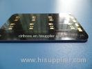
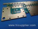
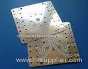
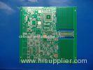
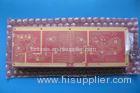
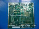
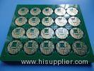
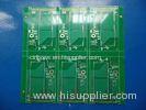
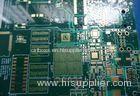
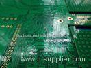
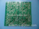
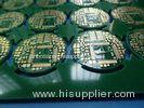
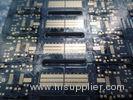
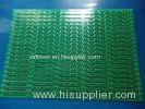
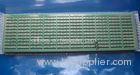
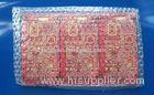
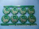
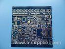
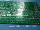
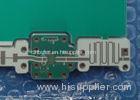
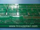
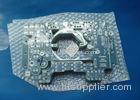
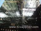
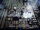
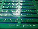
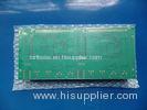
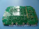
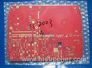
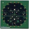
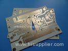
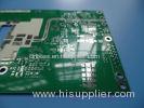
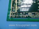
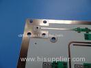
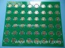
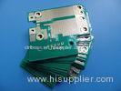
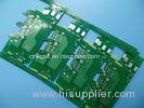
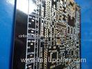
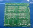
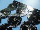
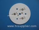
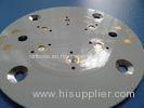
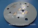
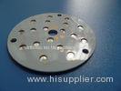
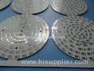
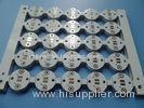
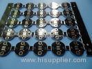
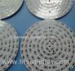
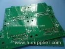
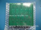
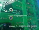
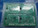
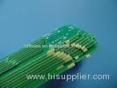
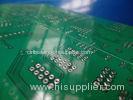
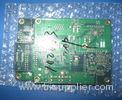
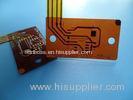
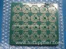
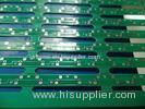
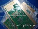
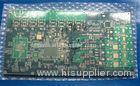
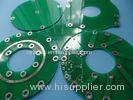
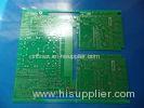
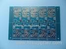
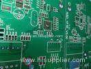
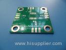
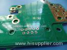
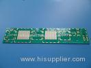
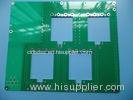
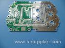
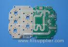
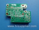
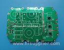
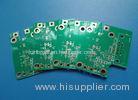
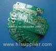
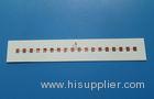
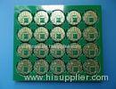
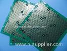
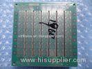
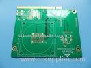
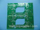
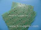
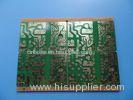
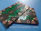
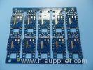
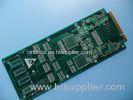
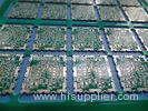
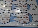
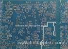
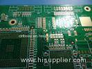
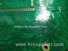
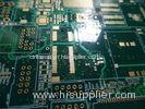
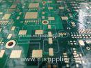
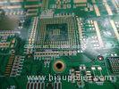
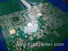
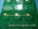
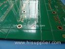
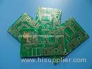
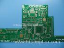
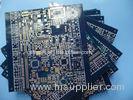
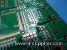
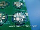
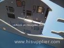
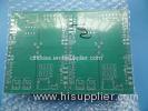
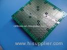
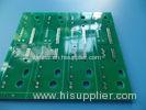
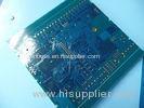
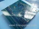
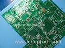
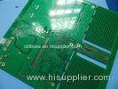
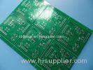
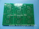
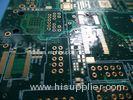
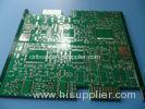
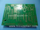
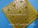
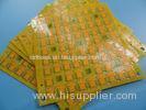
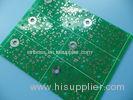
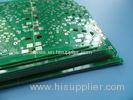
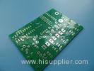
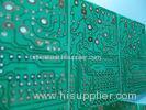
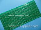
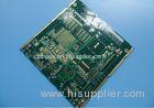
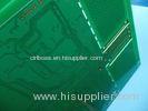
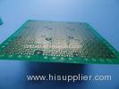
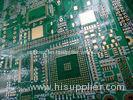
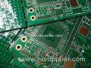
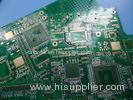
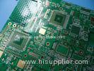
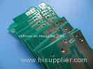
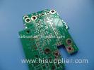
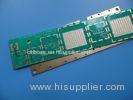
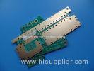
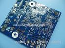
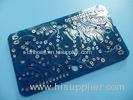
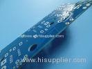
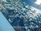
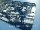
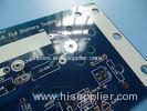
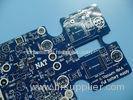
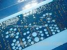
Yellow Mask 0.6mm Via In Pad PCB 6 Layer For Bluetooth Transmitter
| Place of Origin: | Zhejiang, China (Mainland) |
|
|
|
| Add to My Favorites | |
| HiSupplier Escrow |
Product Detail
Yellow Mask 0.6mm Via In Pad PCB 6 Layer For Bluetooth Transmitter
PCB paramters
<table border="1" c
Yellow Mask 0.6mm Via In Pad PCB 6 Layer For Bluetooth Transmitter
PCB paramters
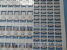
| PCB SIZE | 110 x 105mm=76PCS |
| BOARD TYPE | |
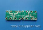
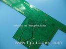
| Number of Layers | Multilayer, 6 layer PCB |
| Surface Mount Components | YES |
| Through Hole Components | NO |
| LAYER STACKUP | copper ------- 18um(0.5oz)+plate TOP CS |
| 4mil prepreg | |
| copper ------- 18um(0.5oz) GND Plane | |
| 5mil FR-4 | |
| copper ------- 18um(0.5oz) PWR Plane | |
| 4mil prepreg | |
| copper ------- 18um(0.5oz) PWR Plane | |
| 4mil FR-4 | |
| copper ------- 18um(0.5oz) SIG | |
| 4mil prepreg | |
| copper ------- 18um(0.5oz) BOT PS | |
| TECHNOLOGY | |
| Minimum Trace and Space: | 3mil/4mil |
| Minmum / Maximum Holes: | 0.25/3.50mm |
| Number of Different Holes: | 27 |
| Number of Drill Holes: | 3011 |
| Number of Milled Slots: | 0 |
| Number of Internal Cutouts: | 0 |
| Impedance Control | no |
| BOARD MATERIAL | |
| Glass Epoxy: | FR-4, ITEQ IT140 TG>135, er<5.4 |
| Final foil external: | 1oz |
| Final foil internal: | 0.5oz |
| Final height of PCB: | 0.6mm ±0.1 |
| PLATING AND COATING | |
| Surface Finish | Immersion gold 0.025µm over 3µm Nickel (9.4% area) |
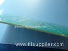
| Solder Mask Apply To: | TOP and Bottom, 12micron Minimum |
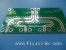
| Solder Mask Color: | Yellow |
| Solder Mask Type: | LPSM |
| CONTOUR/CUTTING | Routing |
| MARKING | |
| Side of Component Legend | No silkscreen requried. |
| Colour of Component Legend | No silkscreen requried. |
| Manufacturer Name or Logo: | No silkscreen requried. |
| VIA | Plated through hole(PTH), Via in Pad and via capping on CS and PS, vias not be visible. |
| FLAMIBILITY RATING | UL 94-V0 Approval MIN. |
| DIMENSION TOLERANCE | |
| Outline dimension: | 0.0059" |
| Board plating: | 0.0029" |
| Drill tolerance: | 0.002" |
| TEST | 100% Electrical Test prior shipment |
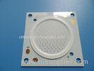
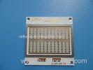
| APPLICATION: | Bluetooth Transmitter |
| TYPE OF ARTWORK TO BE SUPPLIED | email file, Gerber RS-274-X, PCBDOC etc |
| SERVICE AREA | Worldwide, Globally. |
Advantages
a) UL94V0 FR-4 Think laminates.
b) RoHS compliant and suitable for thermal reliability needs,and Lead free assemblies with a maximum reflow temperature of 260
c) Immersion gold PCB. SMT process is resistant to reflow soldering, resistant to rework.
d) ISO certified PCB manufacturing factory.
e) Meeting your printed circuit board needs from PCB prototyping to mass volume production.
More Applications in Electronics
Intercom
Phone Tracker
Wifi Repeater
Codec
Surveillance
Design for Manufacture (5)
| Serial NO. | Procedure | Item | Manufacturing capability | ||
| Large volume (S<100 m²) | Middle volume (S<10 m²) | Prototype(S<1m²) | |||
| 84 | Special tolerance | Board thickness of flying probe test | 0.6-4.0mm | ||
| 85 | Panel size of flying probe test | Size≤900X600mm,Small size can be compensated through manufacturing procedure | |||
| 86 | Panel size of fixture test method | Size≤460X380mm, Small size can be compensated through manufacturing procedure | |||
| 87 | Board thickness of fixture test method | 0.4-6.0mm | |||
| 88 | Tolerance of press-fit hole | ±2mil | |||
| 89 | Tolerance of NPTH | ±2mil | |||
| 90 | Tolerance of PCB thickness | 1.0mm≥PCB thickness, Tolerance ±0.1mm1.0mm≤PCB thickness, Tolerance ±10% | |||
| 91 | Tolerance of depth of countersunk hole | ±0.2mm | |||
| 92 | Depth tolerance of blind slot | ±0.2mm | |||
| 93 | Maximum shipment size | Size≤1200X600mm(Double side, no test required) | |||
| 94 |
Related SearchFind more related products in following catalogs on Hisupplier.comCompany InfoBICHENG ENTERPRISE LIMITED [China (Mainland)]
Business Type:Manufacturer You May Like:
Printable Page
Bookmark this page
Sitemap XML About HiSupplier Help Center Customer Service Friend Links Site Map Archives Browse by: China Suppliers - Hot Products - Products Directory - Offers Directory - Suppliers Directory - Buyers Directory Language Option: العربية - Nederlands- Français- Deutsch- Italiano- 日本語- 한국의- Português- Pусский- Español Copyright © HiSupplier.com Online Inc. All Rights Reserved.

| ||||