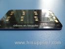
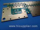
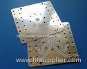
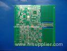
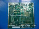
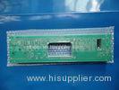
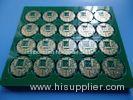
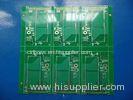
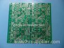
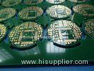
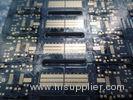
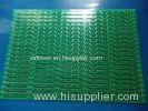
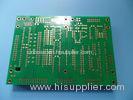
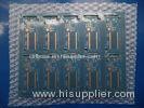
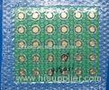
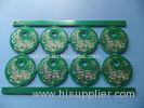
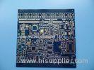
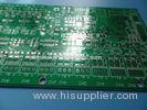
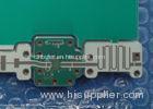
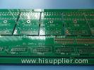
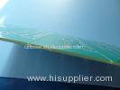
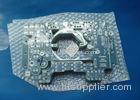
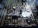
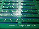
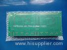
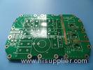
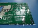
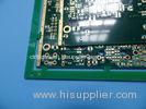
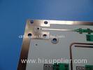
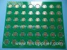
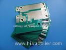
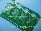
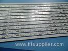
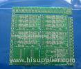
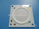
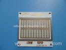
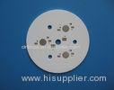
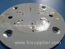
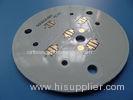
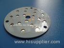
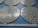
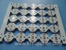
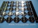
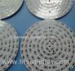
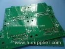
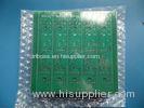
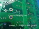
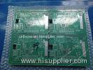
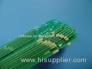
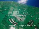
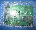
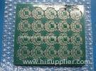
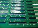
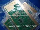
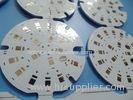
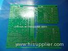
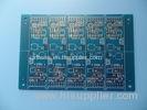
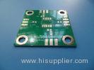
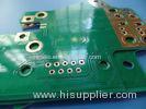
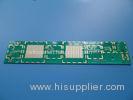
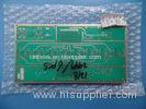
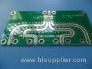
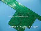
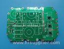
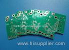
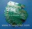
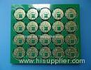
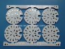
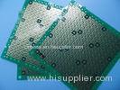
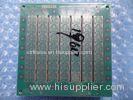
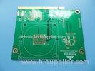
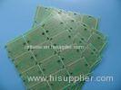
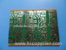
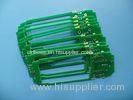
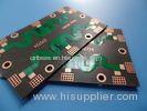
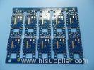
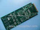
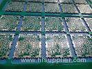
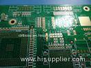
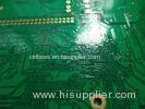
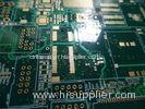
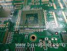
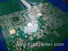
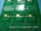
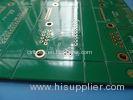
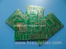
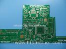
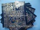
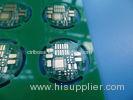
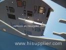
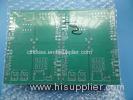
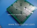
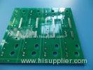
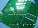
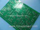
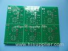
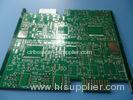
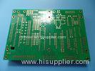
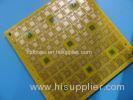
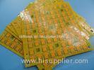
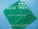
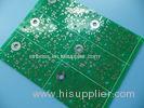
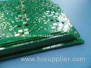
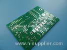
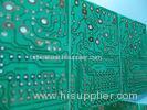
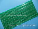
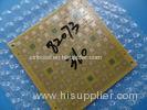
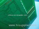
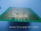
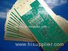
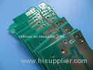
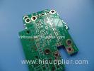
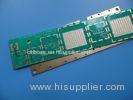
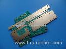
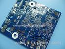
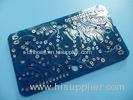
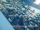
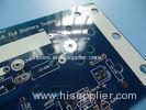
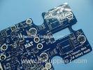
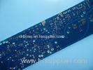
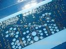
White Solder Mask Double Layer PCB HASL 1.6mm Printed Circuit Assembly
| Place of Origin: | Zhejiang, China (Mainland) |
|
|
|
| Add to My Favorites | |
| HiSupplier Escrow |
Product Detail
White Solder Mask Double Layer PCB HASL 1.6mm Printed Circuit Assembly PCB data sheets<table border="1" cellpadding="0" c
White Solder Mask Double Layer PCB HASL 1.6mm Printed Circuit Assembly
PCB data sheets
| PCB SIZE | 210 x 202mm=2 designs = 9PCS |
| BOARD TYPE | |
| Number of Layers | Double Sided PCB, 2 layer PCB |
| Surface Mount Components | YES |
| Through Hole Components | NO |
| LAYER STACKUP | copper ------- 18um(0.5 oz)+plate TOP layer |
| FR-4 1.5mm | |
| copper ------- 18um(0.5 oz)+plate BOT Layer | |
| TECHNOLOGY | |
| Minimum Trace and Space: | 5.8mil/5.4mil |
| Minmum / Maximum Holes: | 0.3/3.3mm |
| Number of Different Holes: | 9 |
| Number of Drill Holes: | 1245 |
| Number of Milled Slots: | 21 |
| Number of Internal Cutouts: | 1 |
| Impedance Control: | no |
| Number of Gold finger: | 0 |
| BOARD MATERIAL | |
| Glass Epoxy: | FR-4 TG135, CTI 175V-249V, er<5.4. Shengyi Supplied |
| Final foil external: | 1oz |
| Final foil internal: | 0oz |
| Final height of PCB: | 1.6mm ±0.16 |
| PLATING AND COATING | |
| Surface Finish | Hot Air Soldering Leveling(HASL), Sn>=2.54µm |
| Solder Mask Apply To: | TOP and Bottom, 12micron Minimum |
| Solder Mask Color: | White, PSR400 WT02, Taiyo Supplied |
| Solder Mask Type: | LPSM |
| CONTOUR/CUTTING | Routing |
| MARKING | |
| Side of Component Legend | TOP |
| Colour of Component Legend | Black |
| Manufacturer Name or Logo: | Marked on the board in a conductor and leged FREE AREA |
| VIA | Plated through hole(PTH), via tented. |
| FLAMIBILITY RATING | UL 94-V0 Approval MIN. |
| DIMENSION TOLERANCE | |
| Outline dimension: | 0.0059" |
| Board plating: | 0.0029" |
| Drill tolerance: | 0.002" |
| TEST | 100% Electrical Test prior shipment |
| APPLICATION: | Rack rails |
| TYPE OF ARTWORK TO BE SUPPLIED | email file, Gerber RS-274-X, PCBDOC etc |
| SERVICE AREA | Worldwide, Globally. |
Advantages
a) FR-4 Tg135 HASL PCB
b) Engineering design prevents problems from occurring in pre production.
c) Meeting your printed circuit board needs from PCB prototyping to mass volume production.
d) ISO certified PCB manufacturing factory.
e) DDU Door to door shipment with competitive shipping cost. You don’t need to arrange anything after confirming the order. Just wait for your PCB delivery to your hand.
More Applications in Electronics
Wireless Router Range
Inveter
Power Invertor
3G USB Dongle
Electricity Converter
Performance parameter of MCPCB substrate (The parameter will continue to be improved without notice)
| Test item | Unit | Aluminum base | Copper base | Iron base | Test method |
| Actual vale | Actual vale | Actual vale | |||
| Peel strength | N/mm | 2.2 | 2 | 2.3 | 4010 of GJB1651 |
| Surface resistance | MΩ | 1 x (10^6) | 1 x (10^6) | 1 x (10^6) | 5020 of GJB1651 |
| Volume resistance | MΩ.m | 3.2 x (10^7) | 3.2 x (10^7) | 3.2 x (10^7) | 5020 of GJB1651 |
| Breakdown voltage | KV/min | ≥2.0 (Breakdown voltage is adjustable according to customers' demend) | ≥1.0 (Breakdown voltage is adjustable according to customers' demend) | ≥1.0 (Breakdown voltage is adjustable according to customers' demend) | 5040 of GJB1651 |
| Solder dipping | /min | 260, 3 minutes, no bubble and delamination | 260, 3 minutes, no bubble and delamination | 260, 3 minutes, no bubble and delamination | 4010 of GJB1651 |
| Flammability | - | FV-0 | FV-0 | FV-0 | 17 of GB/T4722 |
| Thermal resistance | /W | 0.25-1.2 | 0.25-1.2 | 0.25-1.2 | TO-220 |
| Dielectric constant | - | 3 | 3 | 3 | (40,93%,96h) |
| Thermal conductivity of Dielectric | W/M.K | 0.8-8 | 0.8-350 | 0.8-3 | ASTM 5470-D |
| Working temperature | ≤120 | ≤120 | ≤120 | (40,93%,1Y) | |
| Thermal conductivity of metal base | W/M.K | ≥200 | ≥350 | ≥45 | ASTM |
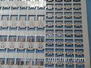
Reference drill table and contour fabricating drawing
FAQ
What's your minimum isolation of layers?
The minimum thickness of prepreg in inner layer is 0.06mm for prototypes, and thicker at 0.1mm for mass production.
Related Search
Find more related products in following catalogs on Hisupplier.com
Related Products
-
Solar Panel 580W for solar system high efficient N-type Monocrystalline Silicon CellsJK580,JK585,JK590,JK595,JK600,JK605

-
Solar Panel 580W for solar system high efficient N-type Monocrystalline Silicon CellsJK580,JK585,JK590,JK595,JK600,JK605

Company Info
BICHENG ENTERPRISE LIMITED [China (Mainland)]
Business Type:Manufacturer
City: Shenzhen
Province/State: Guangdong
Country/Region: China (Mainland)


