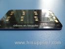
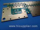
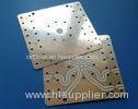
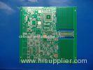
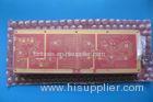
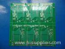
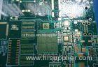
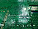
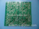
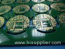
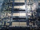
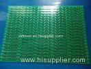
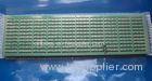
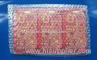
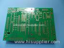
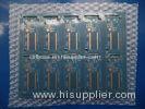
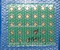
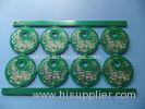
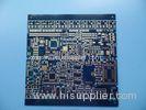
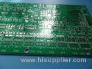
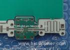
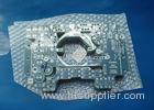
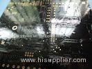
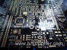
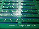
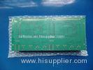
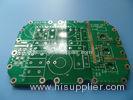
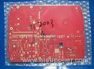
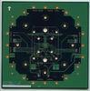
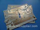
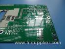
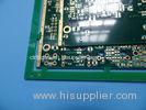
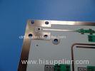
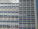
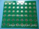
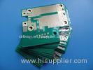
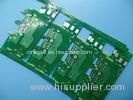
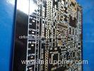
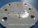
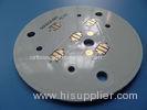
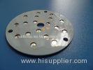
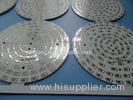
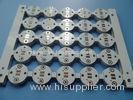
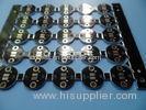
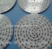
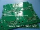
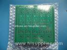
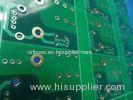
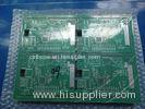
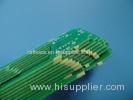
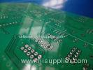
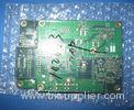
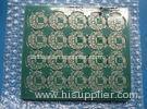
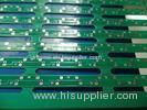
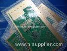
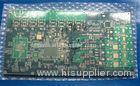
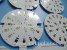
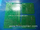
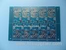
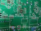
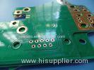
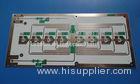
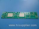
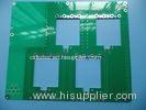
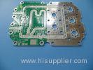
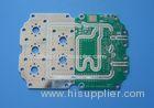
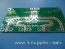
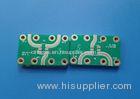
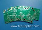
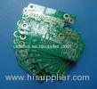
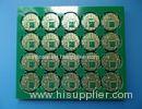
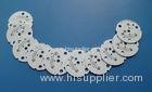
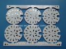
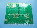
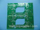
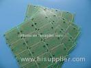
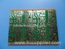
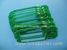
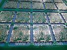
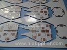
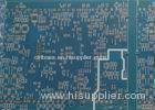
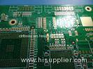
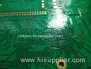
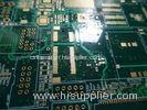
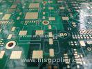
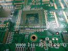
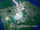
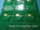
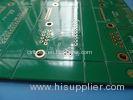
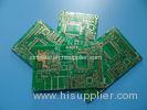
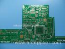
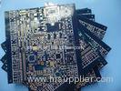
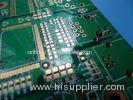
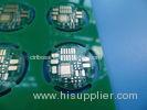
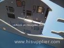
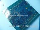
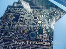
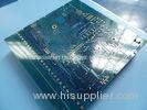
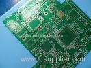
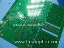
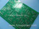
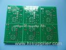
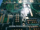
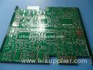
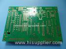
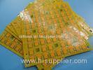
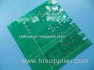
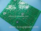
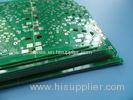
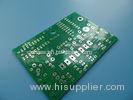
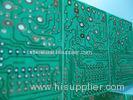
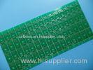
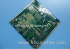
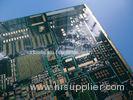
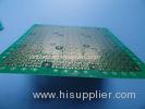
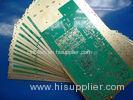
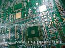
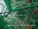
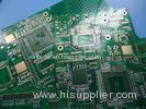
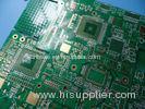
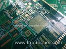
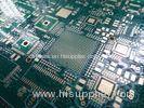
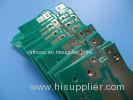
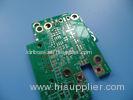
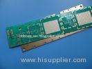
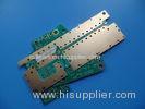
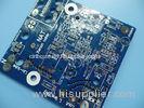
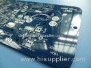
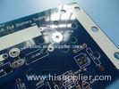
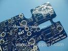
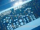
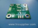
Low Loise Amplifier High Speed Circuit Design High Density Interconnect PCB
| Place of Origin: | Zhejiang, China (Mainland) |
|
|
|
| Add to My Favorites | |
| HiSupplier Escrow |
Product Detail
Low Loise Amplifier High Speed Circuit Design High Density Interconnect PCB
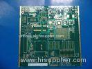
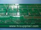
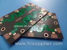
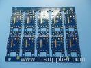
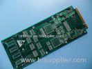
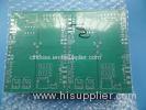
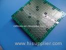
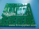
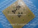
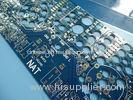
PCB parameter
<table bor
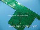
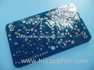
Low Loise Amplifier High Speed Circuit Design High Density Interconnect PCB
PCB parameter
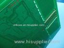
| PCB SIZE | 60 x 54mm=1PCS |
| BOARD TYPE | |
| Number of Layers | Double sided PCB |
| Surface Mount Components | YES |
| Through Hole Components | NO |
| LAYER STACKUP | copper ------- 35um(1oz)+plate TOP layer |
| RO4350B 20mil (0.508mm) | |
| copper ------- 35um(1oz)+plate BOT Layer | |
| TECHNOLOGY | |
| Minimum Trace and Space: | 7.5mil/8.8mil |
| Minmum / Maximum Holes: | 0.5/3.2mm |
| Number of Different Holes: | 5 |
| Number of Drill Holes: | 191 |
| Number of Milled Slots: | 0 |
| Number of Internal Cutouts: | 0 |
| Impedance Control | NO |
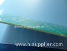
| BOARD MATERIAL | |
| Glass Epoxy: | RO4350B 20mil (0.508mm), Tg 288 |
| Final foil external: | 1.5oz |
| Final foil internal: | 0oz |
| Final height of PCB: | 0.6-0.7mm |
| PLATING AND COATING | |
| Surface Finish | Electroless Nickle over Immersion Gold (ENIG)( 1 µ" over 100 µ" nickle) |
| Solder Mask Apply To: | Top and Bottom, 12micon Minimum. |
| Solder Mask Color: | Green, PSR-2000GT600D, Taiyo supplied. |
| Solder Mask Type: | LPSM |
| CONTOUR/CUTTING | Routing |
| MARKING | |
| Side of Component Legend | TOP |
| Colour of Component Legend | White, IJR-4000 MW300, Taiyo Supplied. |
| Manufacturer Name or Logo: | Marked on the board in a conductor and leged FREE AREA |
| VIA | Plated Through Hole(PTH) |
| FLAMIBILITY RATING | UL 94-V0 Approval MIN. |
| DIMENSION TOLERANCE | |
| Outline dimension: | 0.0059" (0.15mm) |
| Board plating: | 0.0030" (0.076mm) |
| Drill tolerance: | 0.002" (0.05mm) |
| TEST | 100% Electrical Test prior shipment |
| APPLICATION: | Low noise amplifier (LNA) |
| TYPE OF ARTWORK TO BE SUPPLIED | email file, Gerber RS-274-X, PCBDOC etc |
| SERVICE AREA | Worldwide, Globally. |
Advantages
a) RO4350B substrate. Excellent high frequency performance due to low dielectric tolerance and loss.
b) Stable electrical coefficient of dielectric constant.
c) PCB manufacturing on required specifications. Right manufacturing instruction (MI), comprehensive equipment management and maintenance and process control, strict WIP inspection and monitoring as well as working instruction, all those make the whole fabrication process totally controlled.
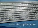
d) Meeting your printed circuit board needs from PCB prototyping to mass volume production.
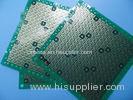
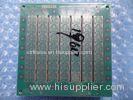
More Applications in Electronics
AC Inverter
Wifi Antenna Booster
Wireless Broadband Router
Modem GSM
USB Adaptor
Hdmi Splitter
Switch Mode Power Supply
Memory Module
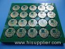
Consumer and Multilayer PCB
Game Player
PCB knowledge: ENIG
ENIG stands for Electroless nickel immersion gold which is a type of surface plating used for circuit boards. It consists of an electroless nickel plating covered with a thin layer of immersion gold. Normally, the thickness of nickel is 120µ” - 200µ” (3µm to 5µm ) and gold 1-5µ” (0.025µm – 0.127µm).
ENIG has several advantages than HASL, including
a) Excellent surface planarity, particularly helpful for PCBs with BGA packages or even CSP mounted components to reduce failure rate during assembly and soldering.
b) Good oxidation resistance and good heat dissipation.
c) Long storage time ( It can be stored for more than 1 year in vacuum bag)
d) High solderability, no stressing of circuit boards and less contamination of PCB surface.
e) SMT process is resistant to reflow soldering, resistant to rework.

FAQ
Do you sell rigid-flex PCB?
Sorry. We currently do not offer rigid-flex PCB.
Related Search
Find more related products in following catalogs on Hisupplier.com
Company Info
BICHENG ENTERPRISE LIMITED [China (Mainland)]
Business Type:Manufacturer
City: Shenzhen
Province/State: Guangdong
Country/Region: China (Mainland)