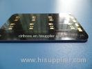
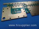
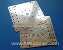
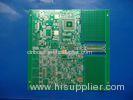
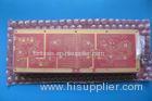
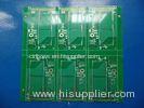
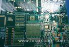
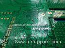
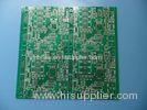
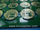
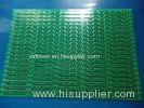
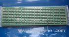
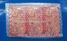
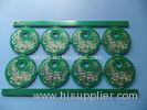
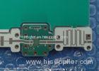
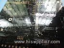
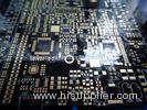
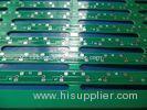
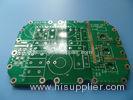
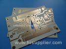
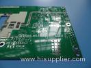
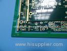
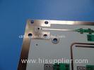
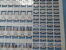
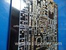
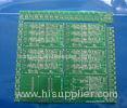
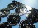
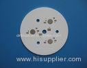
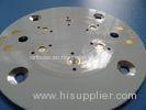
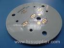
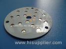
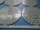
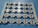
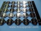
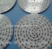
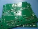
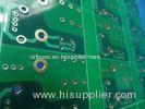
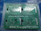
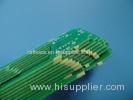
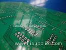
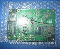
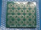
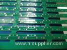
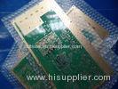
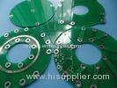
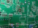
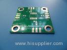
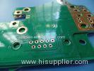
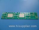
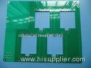
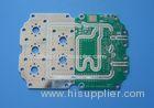
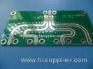
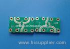
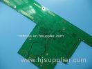
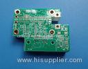
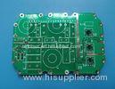
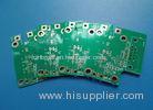
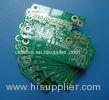
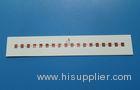
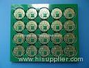
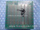
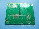
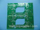
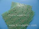
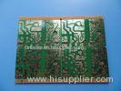
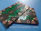
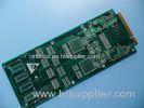
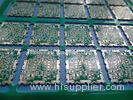
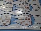
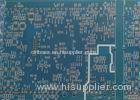
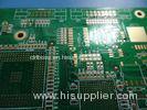
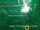
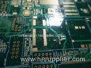
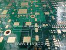
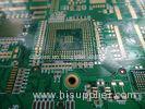
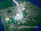
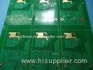
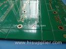
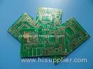
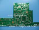
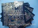
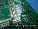
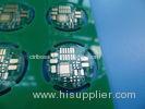
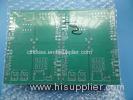
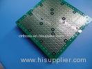
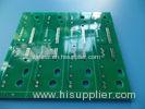
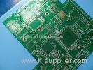
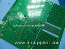
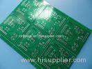
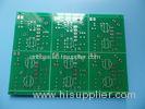
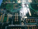
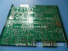
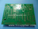
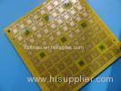
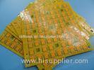
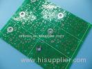
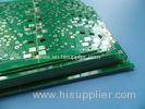
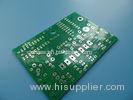
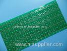
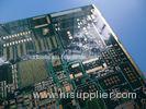
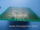
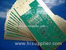
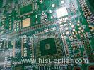
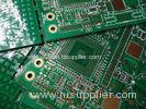
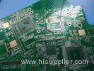
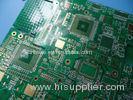
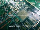
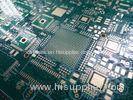
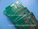
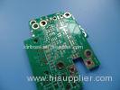
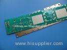
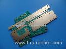
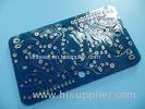
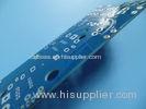
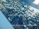
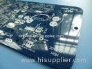
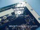
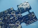
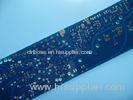
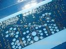
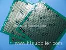
Green FR4 Thin 0.4mm 0.5oz Copper Via In Pad PCB For Wifi Module
| Place of Origin: | Zhejiang, China (Mainland) |
|
|
|
| Add to My Favorites | |
| HiSupplier Escrow |
Product Detail
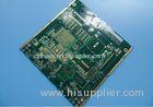
Green FR4 Thin 0.4mm 0.5oz Copper Via In Pad PCB For Wifi Module
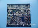
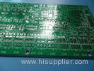
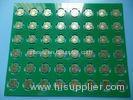
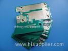
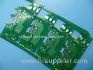
PCB parameters
<table border="1" ce
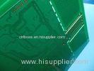
Green FR4 Thin 0.4mm 0.5oz Copper Via In Pad PCB For Wifi Module
PCB parameters
| PCB SIZE | 100 x 100mm=1PCS |
| BOARD TYPE | |
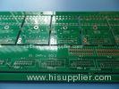
| Number of Layers | Multilayer, 4 layer PCB |
| Surface Mount Components | YES |
| Through Hole Components | NO |
| LAYER STACKUP | copper ------- 18um(0.5oz)+plate TOP |
| 4mil prepreg | |
| copper ------- 18um(0.5oz) GND | |
| 4mil FR-4 | |
| copper ------- 18um(0.5oz) PWR | |
| 4mil prepreg | |
| copper ------- 18um(0.5oz) | |
| TECHNOLOGY | |
| Minimum Trace and Space: | 4mil/4mil |
| Minmum / Maximum Holes: | 0.3/1.50mm |
| Number of Different Holes: | 18 |
| Number of Drill Holes: | 1621 |
| Number of Milled Slots: | 0 |
| Number of Internal Cutouts: | 0 |
| Impedance Control | no |
| BOARD MATERIAL | |
| Glass Epoxy: | ITEQ IT140 TG>135, er<5.4 |
| Final foil external: | 1oz |
| Final foil internal: | 0.5oz |
| Final height of PCB: | 0.4mm ±0.1 |
| PLATING AND COATING | |
| Surface Finish | Immersion gold 0.05µm over 3µm Nickel, (29% area) |
| Solder Mask Apply To: | TOP and Bottom, 12micron Minimum |
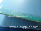
| Solder Mask Color: | Gloss Green, Taiyo PSR-2000GT600D |
| Solder Mask Type: | LPSM |
| CONTOUR/CUTTING | Routing |
| MARKING | |
| Side of Component Legend | No silkscreen requried. |
| Colour of Component Legend | No silkscreen requried. |
| Manufacturer Name or Logo: | No silkscreen requried. |
| VIA | Plated through hole(PTH), Via in Pad. |
| FLAMIBILITY RATING | UL 94-V0 Approval MIN. |
| DIMENSION TOLERANCE | |
| Outline dimension: | 0.0059" |
| Board plating: | 0.0029" |
| Drill tolerance: | 0.002" |
| TEST | 100% Electrical Test prior shipment |
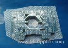
| APPLICATION: | Wifi module |
| TYPE OF ARTWORK TO BE SUPPLIED | email file, Gerber RS-274-X, PCBDOC etc |
| SERVICE AREA | Worldwide, Globally. |
Advantages
a) 4 layer thin PCB for GPS application.
b) Customer complaint rate: <1%
c) PCB manufacturing on required specifications. Right manufacturing instruction (MI), comprehensive equipment management and maintenance and process control, strict WIP inspection and monitoring as well as working instruction, all those make the whole fabrication process totally controlled.
d) Devlivery on time: >98%
e) DDU Door to door shipment with competitive shipping cost.
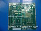
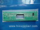
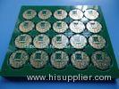
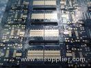
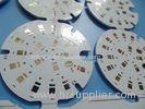
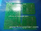
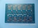
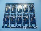
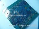
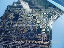
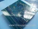
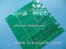
More Applications in Electronics
Tracker Car
Tracking GPS
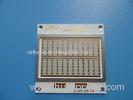
Embedded PC
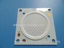
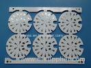
Led Light Panels
Peripheral Device
PCB Knowledge: The components of multilayer PCB --- copper foil
A multilayer board consists of copper foils, thin rigid laminates and prepreg sheets.
The standard thicknesses for copper foils are shown below
| µm | 5 | 9 | 12 | 17.5 | 35 | 70 |
| oz | 0.14 | 0.25 | 0.34 | 0.5 | 1 | 2 |
Thick copper (heavy copper) foils are used for voltage and ground planes by some electronics companies. Thicknesses up to 210 µm (6 oz) are specified for high voltage coil boards. For very fine-line boards, 5 and 9 µm (0.14 and 0.25 oz.), ultrathin copper foils are also used for the outer layers.
Copper foils are used as copper cladding of the thin laminates used in the inner layers. Such laminates can be delivered with different copper thicknesses on the two sides, for example, 17.5 µm (0.5 oz.) on one side for a signal layer and 35 µm (1 oz.) on the other side for ground or voltage planes.
Copper foils are sometimes used directly as cap foils for the outer layers. In such cases, the copper foils are bonded to the next layers by means of prepreg and form the outer layer circuits.
For signal outer layers, the copper foil thickness is usually 17.5 µm (0.5 oz.) or 35 µm (1 oz.) depending on the minimum track width and spacing. In the case of high-density fine-line boards, 5 or 9 µm (0.14 or 0.25 oz.) ultrathin copper foils can be the only solution to achieve the required high resolution when etching the board.
For signal inner layers, a 35 µm (1 oz.) copper foil is normally chosen. For ground and voltage planes, 35 µm (1 oz.) and 70 µm (2 oz.) copper foils can be used. However, the thicker foil, the more difficult it is to fill the apertures in the planes around the hole wall with epoxy flowing from the prepreg sheets during lamination.

FAQ
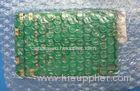
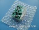
How do you pack the PCBs?
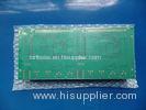
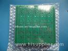
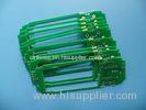
PCBs are packed with Polyethylene air cushion film(vacuum plastic bags) per 20-25 pieces. Pearl cotton (Polyethylene foamed sheet) are put inside carton box.
The hardness of carton box is KK grade(the highest hardness). Maximum gross weight for one carton is less than 12 kgs.
Related Search
Find more related products in following catalogs on Hisupplier.com
Company Info
BICHENG ENTERPRISE LIMITED [China (Mainland)]
Business Type:Manufacturer
City: Shenzhen
Province/State: Guangdong
Country/Region: China (Mainland)