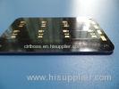
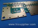
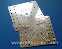
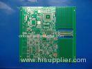
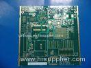
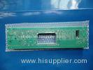
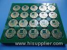
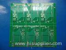
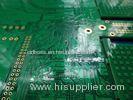
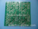
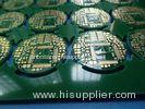
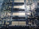
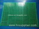
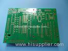
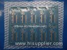
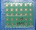
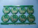
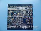
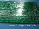
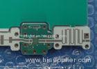
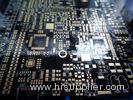
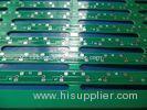
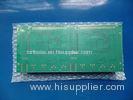
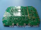
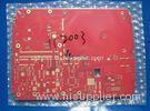
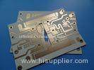
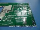
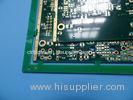
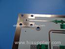
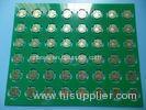
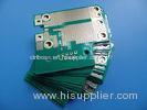
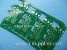
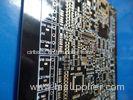
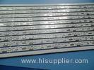
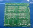
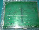
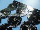
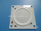
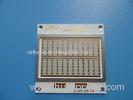
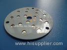
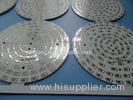
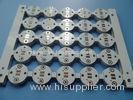
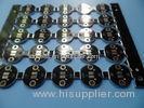
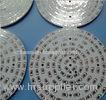
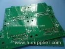
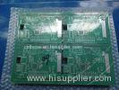
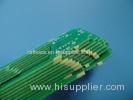
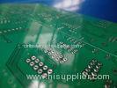
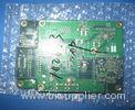
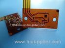
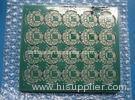
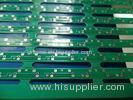
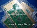
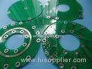
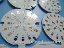
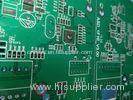
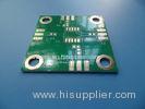
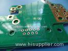
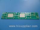
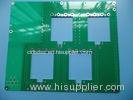
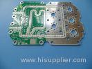
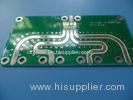
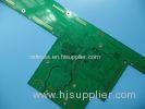
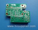
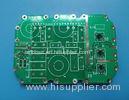
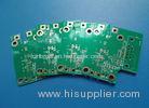
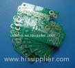
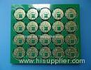
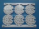
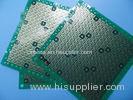
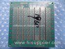
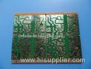
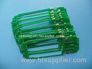
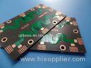
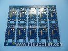
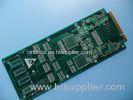
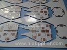
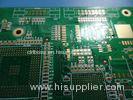
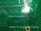
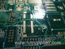
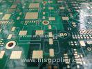
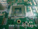
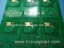
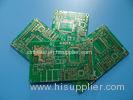
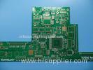
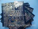
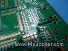
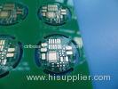
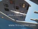
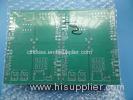
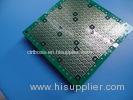
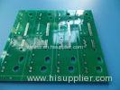
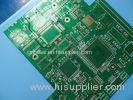
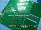
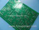
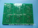
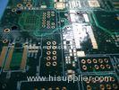
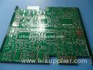
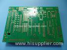
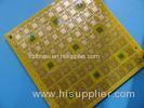
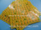
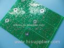
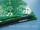
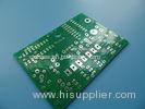
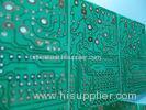
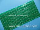
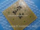
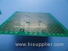
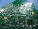
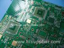
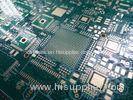
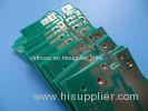
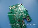
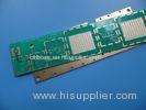
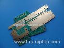
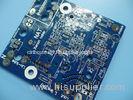
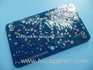
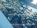
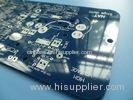
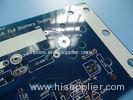
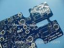
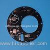
6061 Aluminum Metal Core PCB Single Sided 1W / MK HASL For Power Module
| Place of Origin: | Zhejiang, China (Mainland) |
|
|
|
| Add to My Favorites | |
| HiSupplier Escrow |
Product Detail
6061 Aluminum Metal Core PCB Single Sided 1W / MK HASL For Power Module PCB parameters<table border="1" cellpadding="0" c
6061 Aluminum Metal Core PCB Single Sided 1W / MK HASL For Power Module
PCB parameters
| PCB SIZE | 96 x 96mm=1PCS |
| BOARD TYPE | |
| Number of Layers | Single sided PCB |
| Surface Mount Components | YES |
| Through Hole Components | NO |
| LAYER STACKUP | copper ------- 70um(2oz) |
| 1W/MK dielectric material 75um | |
| Aluminum 6061 1.5mm | |
| TECHNOLOGY | |
| Minimum Trace and Space: | 12mil/20mil |
| Minmum / Maximum Holes: | 3mm / 5.0mm |
| Number of Different Holes: | 12 |
| Number of Drill Holes: | 3 |
| Number of Milled Slots: | 2 |
| Number of Internal Cutouts: | 0 |
| Impedance Control | no |
| BOARD MATERIAL | |
| Aluminum core: | 1W / MK dielectric material 75um |
| Thermal resistance(°C/W) | ≤0.45 |
| Breakdown Voltage(VDC) | 4000 |
| Final foil external: | 1oz |
| Final foil internal: | 0oz |
| Final height of PCB: | 1.6mm ±0.16 |
| PLATING AND COATING | |
| Surface Finish | Hot air soldering leveling(HASL),lead free, Sn>=2.54µm |
| Solder Mask Apply To: | TOP, 12micron Minimum |
| Solder Mask Color: | Black, KSM-S6189BK31 |
| Solder Mask Type: | LPSM |
| CONTOUR/CUTTING | Routing |
| MARKING | |
| Side of Component Legend | TOP |
| Colour of Component Legend | White, IJR-4000 MW300 |
| Manufacturer Name or Logo: | Marked on the board in a conductor and leged FREE AREA |
| VIA | Non Plated Throught Hole (NPTH) |
| FLAMIBILITY RATING | UL 94-V0 Approval MIN. |
| DIMENSION TOLERANCE | |
| Outline dimension: | 0.0059" |
| Board plating: | 0.0029" |
| Drill tolerance: | 0.002" |
| TEST | 100% Electrical Test prior shipment |
| APPLICATION: | Power module |
| TYPE OF ARTWORK TO BE SUPPLIED | email file, Gerber RS-274-X, PCBDOC etc |
| SERVICE AREA | Worldwide, Globally. |
Advantages
a) Aluminum base PCB. Effective heat dissipation reduces the operating temperature of the module, prolonging the service life. Power density and reliability are improved.
b) Reduce the dependence of heat sinks and other hardware (including thermal interface materials), reduce the volume of the product, reduce the cost of hardware and assembly.
c) ISO certified PCB manufacturing factory.
d) Meeting your printed circuit board needs from PCB prototyping to mass volume production.
More Applications in Electronics
Switch LAN
Embedded Systems
Car Tracking System
Led Light Kits
Vehicle GPS
PCB knowledge: The components of multilayer PCB --- Prepreg
A multilayer board consists of copper foils, thin rigid laminates and prepreg sheets.
Prepreg plays a role of bonding material used for bonding the individual thin laminates of the multilayer boards. It consists of glass cloth impregnated with epoxy resin. Unlike rigid laminates, the epoxy resin is only semi-cured. Epoxy resin is referred to as B-stage when semi-cured.
The prepreg sheets are not sticky. During lamination of the board, the epoxy resin is first changed to a liquid state and later in the press cycle to the fully cured state. During the press cycle, the cured epoxy resin in the thin, rigid laminates softens, but it does not become liquid.
Thicknesses of Prepreg sheets
| Glass Fabric Style | Pressed Thickness | Resin Content | |
| mm | mil | % | |
| 7628H(7630) | 0.213 | 8.4 | 50 |
| 7628(43%) | 0.195 | 7.6 | 43 |
| 7628(41%) | 0.185 | 7.3 | 41 |
| 2116HR | 0.135 | 5.3 | 57 |
| 2116 | 0.12 | 4.7 | 52 |
| 2113 | 0.1 | 4 | 56 |
| 1080 | 0.076 | 3 | 64 |
| 1060 | 0.05 | 2 | 71 |
The pressed thickness varies from one manufacturer to another. As long as the PCB designer does not know the brand(s) of the glass fabrics used by the multilayer board manufacturer, it is more or less impossible to specify a detailed build-up. Therefore, this should be left to the manufacturer.
When a board is required impedance control, the thickness of the dielectric material between the individual layers become important and thickness and tolerance are usually specified by designer.
The minimum thickness of the dielectric material (thin laminate or prepreg sheets) is 75 µm (3 mils) and, in some cases, 100 µm (4 mils).
FAQ
Do you offer Mass production?
Yes.We have the independent industrial plant. There're 15000 square meters workshop area. And the brand new automatic equipment were introduced from Israel, Germany,Janpan
and Taiwan area. As of now,the manufacturing capability for 2-12 layer PCBs is 300 thousand square feet per month. 5000 types of different PCBs are shipped to worldwide
each month
Related Search
Find more related products in following catalogs on Hisupplier.com
Company Info
BICHENG ENTERPRISE LIMITED [China (Mainland)]
Business Type:Manufacturer
City: Shenzhen
Province/State: Guangdong
Country/Region: China (Mainland)


