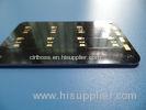
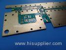
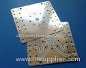
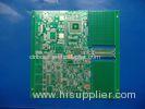
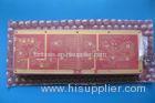
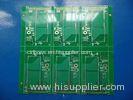
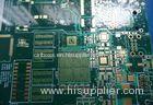
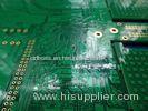
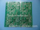
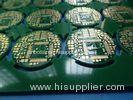
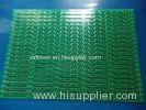
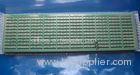
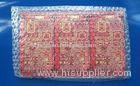
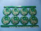
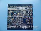
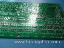
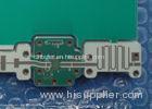
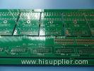
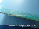
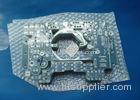
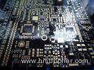
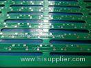
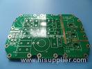
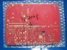
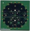
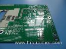
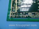
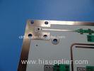
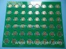
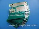
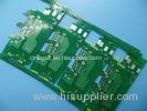
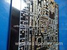
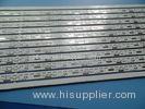
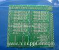
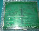
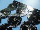
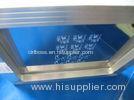
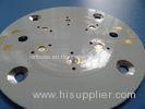
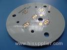
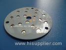
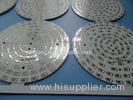
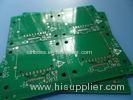
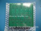
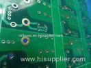
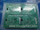
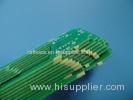
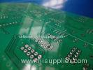
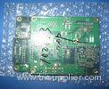
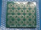
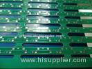
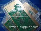
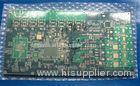
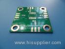
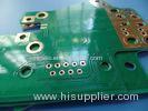
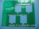
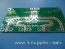
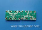
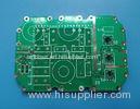
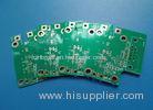
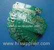
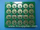
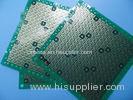
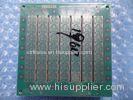
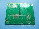
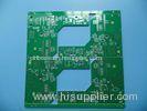
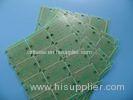
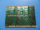
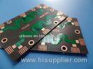
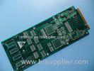
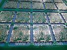
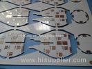
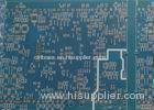
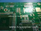
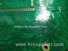
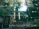
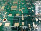
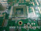
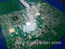
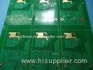
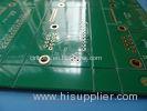
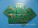
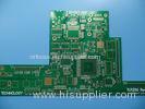
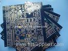
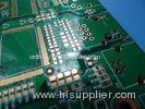
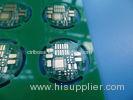
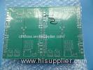
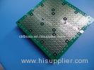
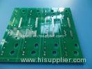
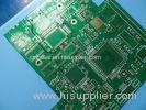
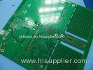
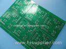
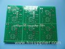
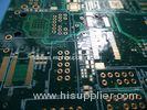
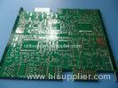
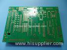
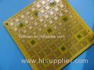
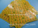
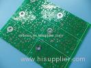
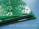
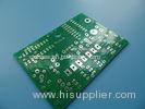
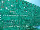
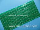
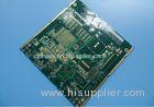
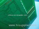
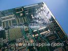
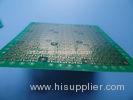
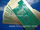
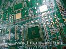
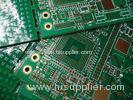
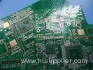
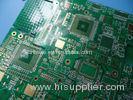
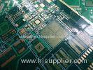
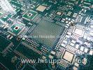
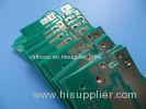
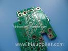
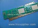
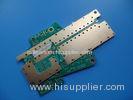
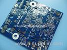
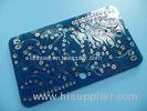
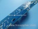
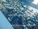
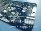
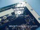
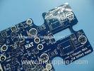
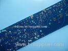
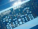
2 Layers High Frequency PCB Ro4350B HASL Pb Free Green PCB Board
| Place of Origin: | Zhejiang, China (Mainland) |
|
|
|
| Add to My Favorites | |
| HiSupplier Escrow |
Product Detail
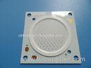
2 Layers High Frequency PCB Ro4350B HASL Pb Free Green PCB Board PCB properties<table border="1" cellpadding="0" cellspac
2 Layers High Frequency PCB Ro4350B HASL Pb Free Green PCB Board
PCB properties
| PCB SIZE | 78 x 61mm=1PCS |
| BOARD TYPE | |
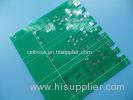
| Number of Layers | Double sided PCB |
| Surface Mount Components | YES |
| Through Hole Components | NO |
| LAYER STACKUP | copper ------- 35um(1oz)+plate TOP layer |
| RO4350B 30mil (0.762mm) | |
| copper ------- 35um(1oz)+plate BOT Layer | |
| TECHNOLOGY | |
| Minimum Trace and Space: | 5.7mil/6.7mil |
| Minmum / Maximum Holes: | 0.6/3.7mm |
| Number of Different Holes: | 3 |
| Number of Drill Holes: | 28 |
| Number of Milled Slots: | 0 |
| Number of Internal Cutouts: | 0 |
| Impedance Control | NO |
| BOARD MATERIAL | |
| Glass Epoxy: | RO4350B 30mil (0.762mm), Tg 288 |
| Final foil external: | 1.5oz |
| Final foil internal: | 0oz |
| Final height of PCB: | 0.8mm ±0.1 |
| PLATING AND COATING | |
| Surface Finish | HASL ,Lead Free, Sn>=2.54µm |
| Solder Mask Apply To: | Top, 12micon Minimum. |
| Solder Mask Color: | Green, PSR-2000GT600D, Taiyo supplied. |
| Solder Mask Type: | LPSM |
| CONTOUR/CUTTING | Routing |
| MARKING | |
| Side of Component Legend | TOP |
| Colour of Component Legend | White, IJR-4000 MW300, Taiyo Supplied. |
| Manufacturer Name or Logo: | Marked on the board in a conductor and leged FREE AREA |
| VIA | Plated Through Hole(PTH), Via tented |
| FLAMIBILITY RATING | UL 94-V0 Approval MIN. |
| DIMENSION TOLERANCE | |
| Outline dimension: | 0.0059" (0.15mm) |
| Board plating: | 0.0030" (0.076mm) |
| Drill tolerance: | 0.002" (0.05mm) |
| TEST | 100% Electrical Test prior shipment |
| APPLICATION: | Multicoupler |
| TYPE OF ARTWORK TO BE SUPPLIED | email file, Gerber RS-274-X, PCBDOC etc |
| SERVICE AREA | Worldwide, Globally. |
Advantages
a) Excellent high frequency performance due to low dielectric tolerance and loss.
b) Lower temperature coefficient of dielectric constant.
c) An Ideal for temperature sensitive applications.
d) DDU Door to door shipment with competitive shipping cost. You don’t need to arrange anything after confirming the order. Just wait for your PCB delivery to your hand.
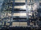
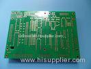
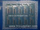
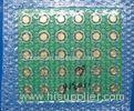
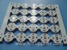
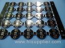
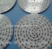
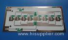
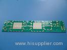
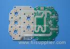
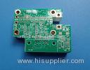
More Applications in Electronics
Meanwell Power Supply
Power Supply Circuit
Power Supply PC
Power Supply Computer
Backup Power Supply
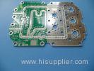
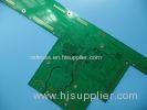
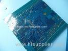
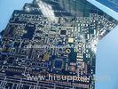
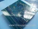
HDI and Multilayer PCB
LNB's for Direct broadcast Satellites
Microstrip and Cellular Base Station Antennas and Power Amplifiers
Spread Spectrum Communications Systems
RF Identifications Tags
PCB knowledge: PCB classification
15.3 Classification (17)
Classification by layers: It's divided into a single sided PCB, double sided PCB and multilayer PCB. The Common multilayer board is generally 4 layers or 6 layers, complex multilayer board up to dozens of layers.
Single Sided PCB
Single Sided Boards are the most basic parts of PCB. Components are concentrated on one side, the wire track is focused on the other side (SMD components and wires for the same side, then the other side of the through-hole components). Because the wire appears only in one side, so this kind of PCB is called single sided.
It has many strict restrictions in the design on the line (because of only one side, each wire must not cross and goes around its own path), so this type of circuit board is used at the early stage of circuit.
Double sided PCB
Both sides of the circuit board are wired, but to use the two sides of the wire, we must have the proper circuit connection between the two sides. The "bridge" between the circuits is called the pilot hole (via). The via is filled with or coated with a small hole in the PCB. It can be connected to the two sides of the wire. Because double sided PCB is twice larger in area than a single sided PCB, it solves the difficulty that wiring staggered in single side PCB (through hole conduction to the other side). It is more suitable for use in circuits that are more complex than a single sided board.
Multilayer PCB
In order to increase the area that can be wired, multilayer board uses more single or double sided wiring board.
PCB using a double side board as inner layer and two pieces of single layer as the outer layer or two double-sided printed circuit board as the inner layer and two pieces of single layer as the outer layer, through the insulation and bonding materials to press each layer together, and the conductive pattern are as per design requirements for interconnection becomes the 4 layers of printed circuit board, 6 layers of printed circuit board, also known as multilayer printed circuit board.
The number of layers of the board does not represent a separate layer of wiring. In particular, the air layer will be joined to control the thickness of the board. Usually the number of layers is even, and contains the outermost 2 layers. Most of the host mainboard is 4 to 8 layers of structure, but the theory can be technically nearly 100 layers of PCB boards. Large supercomputers use quite a lot of layers of mainframe board, but because this kind of computer can be replaced with a lot of ordinary computer clusters, super multilayer board has gradually not been used. Because all of the layers in the PCB are closely combined, it is generally not easy to see the actual number, but if you look carefully at the motherboard, you can also see it.
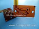
PCB can be also classified by its softness. There’re rigid PCB, flexible PCB and Rigid-flex PCB. Metal core PCB and high frequency PCB are classified by its material.
Multilayer PCB stackup: 6 layer .093" Finish Thickness

FAQ
a) What's your minimum isolation of layers?
The minimum thickness of prepreg in inner layer is 0.06mm for prototypes, and thicker at 0.1mm for mass production.
b) What's your minimum track and spacing?
Actually this depends on the copper weight.
For half oz(18um) copper, it's 3mil / 3.5mil for prototypes, 4mil / 4mil for small production and larger at 5mil / 5mil for mass production.
For 1oz (35um) copper, it's 3mil / 4mil for prototypes, 4mil / 4mil for small production and 5mil / 5mil for mass production.
For 2oz (70um) copper, it's 6mil / 7mil for prototypes, 6mil / 8mil for small production and 7mil / 9mil for mass production.
For 3oz (105um) copper, it's 8mil / 9mil for prototypes, 8mil / 10mil for small production and 9mil /11mil for mass production.
For 4oz (140um) copper, it's 12mil / 11mil for prototypes, 12mil / 12mil for small production and
Related Search
Find more related products in following catalogs on Hisupplier.com
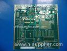
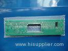
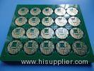
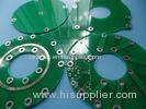
Related Products
.jpg)
.jpg)
.jpg)
.jpg)
.jpg)
.jpg)

Company Info
BICHENG ENTERPRISE LIMITED [China (Mainland)]
Business Type:Manufacturer
City: Shenzhen
Province/State: Guangdong
Country/Region: China (Mainland)