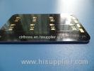
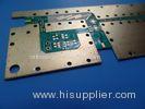
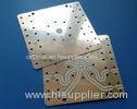
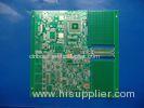
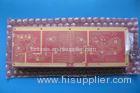
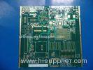
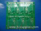
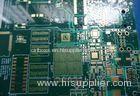
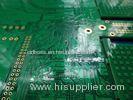
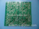
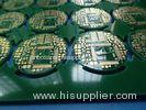
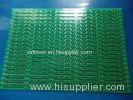
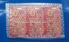
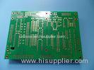
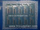
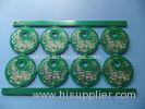
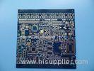
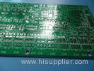
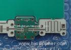
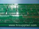
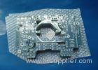
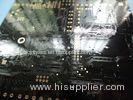
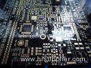
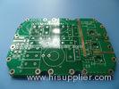
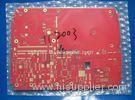
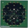
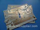
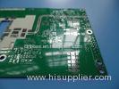
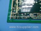
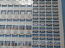
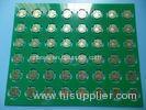
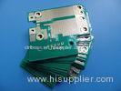
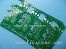
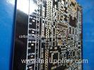
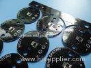
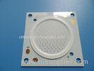
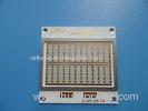
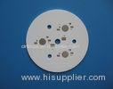
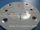
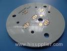
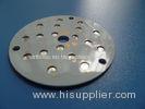
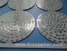
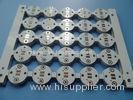
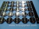
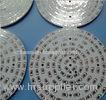
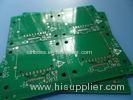
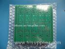
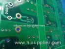
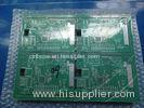
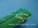
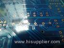
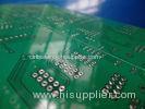
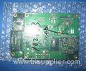
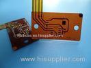
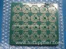
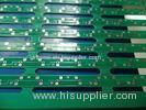
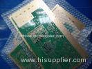
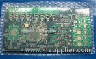
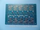
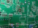
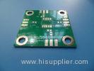
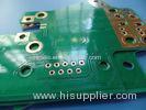
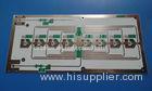
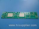
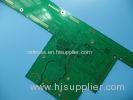
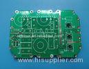
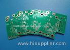
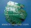
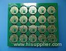
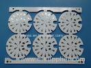
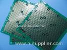
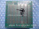
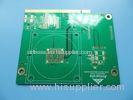
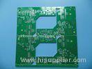
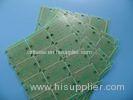
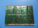
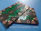
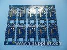
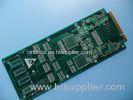
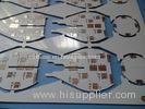
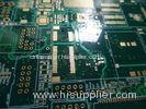
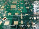
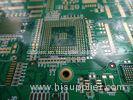
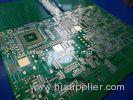
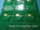
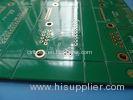
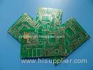
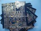
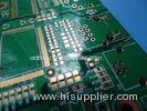
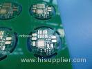
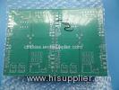
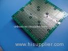
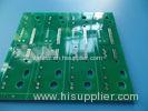
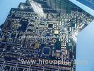
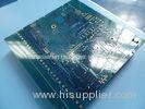
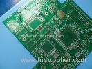
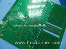
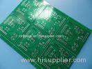
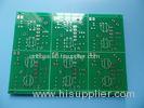
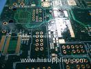
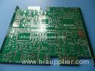
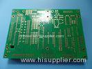
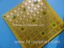
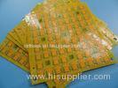
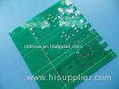
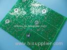
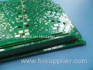
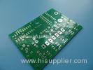
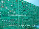
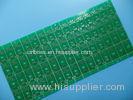
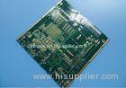
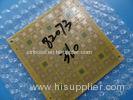
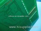
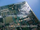
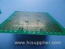
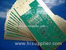
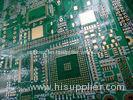
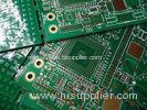
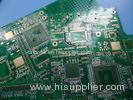
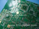
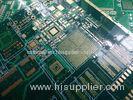
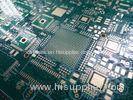
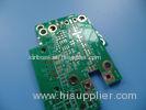
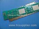
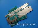
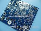
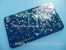
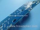
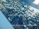
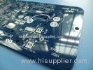
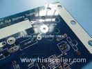
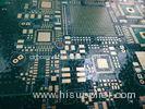
12 Layer BGA Printed Cirucit Board Via In Pad For Programmable Logic Controller
| Place of Origin: | Zhejiang, China (Mainland) |
|
|
|
| Add to My Favorites | |
| HiSupplier Escrow |
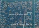
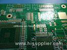
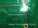
Product Detail
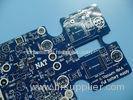
12 Layer BGA Printed Cirucit Board Via In Pad For Programmable Logic Controller
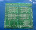
PCB properties
<table bo
12 Layer BGA Printed Cirucit Board Via In Pad For Programmable Logic Controller
PCB properties
| PCB SIZE | 90 x 120mm=1PCS=1design |
| BOARD TYPE | |
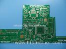
| Number of Layers | Multilayer PCB, 12 Layer PCB |
| Surface Mount Components | YES |
| Through Hole Components | NO |
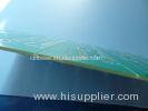
| LAYER STACKUP | copper ------- TOP 17um(1oz)+plate 25um |
| 130 um prepreg 1080 x 2 | |
| copper ------- L02 35um(1oz) | |
| 150um core FR-4 | |
| copper ------- L03 35um(1oz) | |
| 130 um prepreg 1080 x 2 | |
| copper ------- L04 35um(1oz) | |
| 150um core FR-4 | |
| copper ------- L05 35um(1oz) | |
| 130 um prepreg 1080 x 2 | |
| copper ------- L06 35um(1oz) | |
| 150um core FR-4 | |
| copper ------- L07 35um(1oz) | |
| 130 um prepreg 1080 x 2 | |
| copper ------- L08 35um(1oz) | |
| 150um core FR-4 | |
| copper ------- L09 35um(1oz) | |
| 130 um prepreg 1080 x 2 | |
| copper ------- L10 35um(1oz) | |
| 150um core FR-4 | |
| copper ------- L11 35um(1oz) | |
| 130 um prepreg 1080 x 2 | |
| copper ------- BOT 17um(0.5oz)+plate 25um | |
| TECHNOLOGY | |
| Minimum Trace and Space: | 5.5mil/5mil |
| Minmum / Maximum Holes: | 0.25/2.0mm |
| Number of Different Holes: | 25 |
| Number of Drill Holes: | 1552 |
| Number of Milled Slots: | 0 |
| Number of Internal Cutouts: | 0 |
| Impedance Control | NO |
| BOARD MATERIAL | |
| Glass Epoxy: | FR-4, ITEQ IT-140, TG>135, er<5.4 |
| Final foil external: | 1oz |
| Final foil internal: | 1oz |
| Final height of PCB: | 1.924mm ±10% |
| PLATING AND COATING | |
| Surface Finish | Electroless Nickle over Immersion Gold (ENIG)( 2 µ" over 100 µ" nickle) |
| Solder Mask Apply To: | Top and Bottom, 12micon Minimum. |
| Solder Mask Color: | Green, PSR-2000GT600D, Taiyo supplied. |
| Solder Mask Type: | LPSM |
| CONTOUR/CUTTING | Routing |
| MARKING | |
| Side of Component Legend | TOP |
| Colour of Component Legend | White, IJR-4000 MW300, Taiyo Supplied. |
| Manufacturer Name or Logo: | Marked on the board in a conductor and leged FREE AREA |
| VIA | Plated Through Hole(PTH), via tented. Vin in pad under BGA package |
| FLAMIBILITY RATING | UL 94-V0 Approval MIN. |
| DIMENSION TOLERANCE | |
| Outline dimension: | 0.0059" (0.15mm) |
| Board plating: | 0.0030" (0.076mm) |
| Drill tolerance: | 0.002" (0.05mm) |
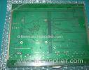
| TEST | 100% Electrical Test prior shipment |
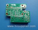
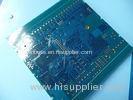
| APPLICATION: | Programmable logic controller |
| TYPE OF ARTWORK TO BE SUPPLIED | email file, Gerber RS-274-X, PCBDOC etc |
| SERVICE AREA | Worldwide, Globally. |
Advantages
a) Engineering design prevents problems from occurring in pre production.
b) Products and Manufacturing are certified by authorized organizations.
c) 100% tests inclusive of electrical test and AOI inspection.High voltage test, Impedance control test, micro-section, solder-ability test, thermal stress test, reliability test, insulation resistance test and ionic contamination test etc.
d) Eligible products rate of first production: >95%
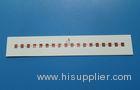
More Applications in Electronics
Wifi Module
Router Switch
Storage Server
GPS USB
Mobile Router
Low Noise Amplifier
LNA
Preamplifier
Splitter
Transmitter
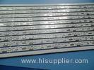
PCB Knowledge: The Difficulty Factors for Multilayer boards
Multilayer PCB’s represent one of the most complicates products in PCB industry. In order to design producible multilayer PCB’s, it is imperative that PCB designers understand the processes and difficulty factors
*Build-up
The more layers in a multilayer PCB’s, the greater risk of mis-registration during laminate process. The difficulty factor, therefore, increase with an increasing layer counts.
*Core thickness of rigid inner laminates
Inner layers are normally based on thin rigid laminate cores with copper cladding. The thinner the rigid laminates, the more difficult they are to handle, for example, in the etching process.
*Thickness tolerance (total thickness inclusive of copper foils)
The difficulty factor and the rejection rate depend very much upon the thickness tolerance required, and indirectly upon the layer build-up. When thickness tolerance T=±10%, obviously rejection ratio trends to zero.

FAQ
How do you control the quality?
We believe engineering design prevents problems from occurring in preproduction. Our PCB and Manufacturing process are certified by authorized organizations.
100% tests are inclusive of electrical test and AOI inspection, high voltage test, impedance control test, micro-section, solder-ability test, thermal stress test,
reliability test, insulat
Related Search
Find more related products in following catalogs on Hisupplier.com
Company Info
BICHENG ENTERPRISE LIMITED [China (Mainland)]
Business Type:Manufacturer
City: Shenzhen
Province/State: Guangdong
Country/Region: China (Mainland)