

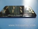
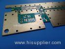
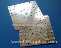
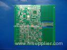
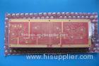
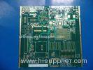
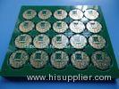
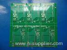
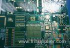
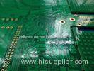
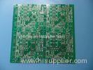
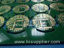
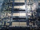
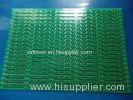
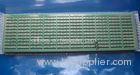
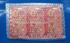
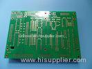
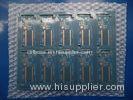
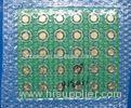
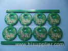
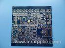
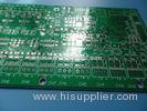
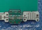
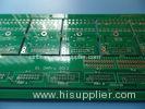
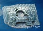
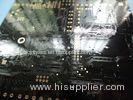
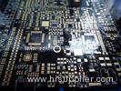
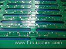
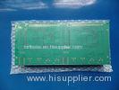
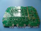
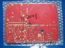
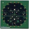
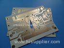
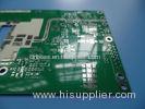
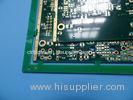
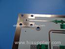
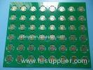
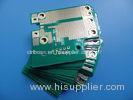
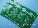
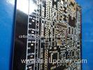
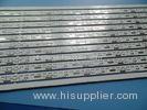
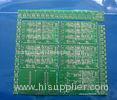
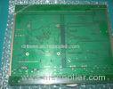
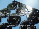
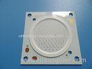
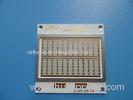
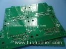
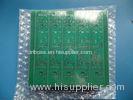
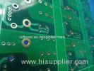
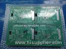
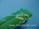
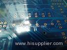
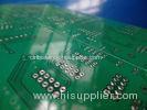
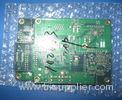
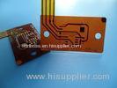
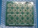
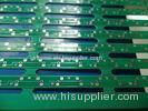
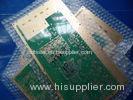
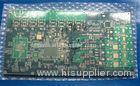
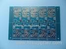
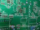
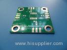
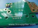
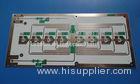
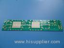
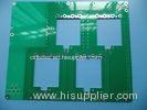
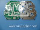
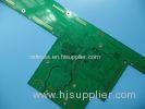
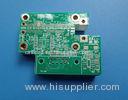
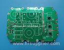
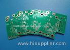
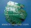
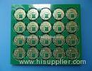
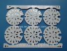
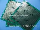
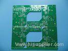
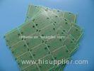
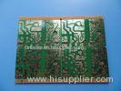
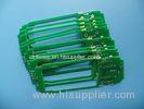
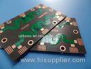
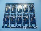
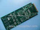
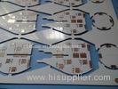
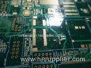
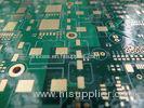
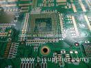
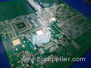
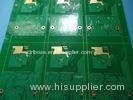
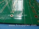
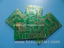
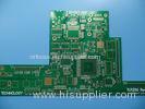
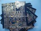
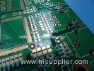
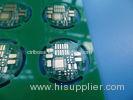
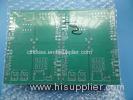
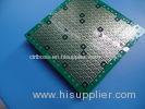
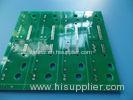
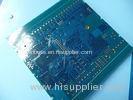
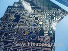
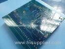
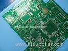
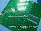
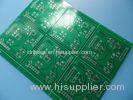
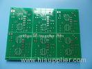
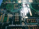
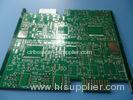
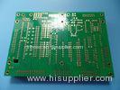
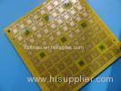
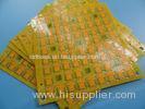
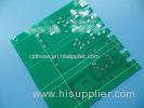
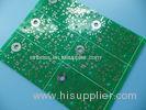
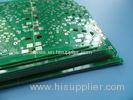
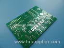
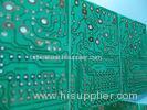
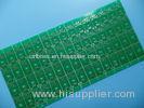
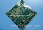
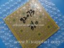
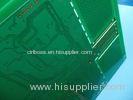
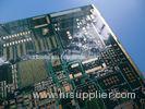
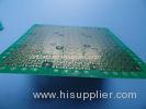
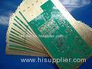
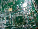
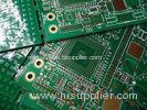
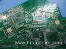
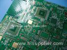
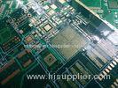
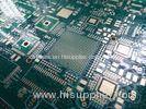
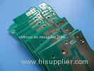
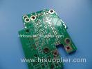
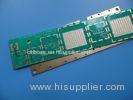
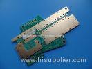
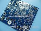
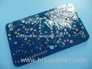
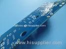
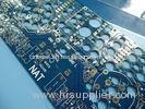
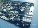
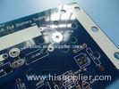
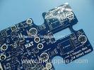
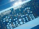
8 Layer High Tg PCB FR4 1.6mm Immersion Gold Multilayer Circuit Board
| Place of Origin: | Zhejiang, China (Mainland) |
|
|
|
| Add to My Favorites | |
| HiSupplier Escrow |
Product Detail
8 Layer High Tg PCB FR4 1.6mm Immersion Gold Multilayer Circuit Board
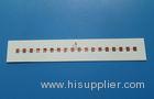
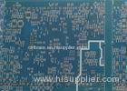
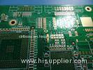
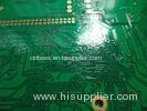
PCB Data Sheets
<table border=
8 Layer High Tg PCB FR4 1.6mm Immersion Gold Multilayer Circuit Board
PCB Data Sheets
| PCB SIZE | 215 x 212mm=1PCS |
| BOARD TYPE | |
| Number of Layers | Multilayer PCB, 8 layer PCB |
| Surface Mount Components | YES |
| Through Hole Components | YES |
| LAYER STACKUP | copper ------- 18um(0.5oz)+plate TOP layer |
| Prepreg 7628 0.195mm | |
| copper ------- 35um(1oz) MidLayer 1 | |
| FR-4 0.2mm | |
| copper ------- 35um(1oz) MidLayer 2 | |
| Prepreg 7628 0.195mm | |
| copper ------- 35um(1oz) MidLayer 3 | |
| FR-4 0.2mm | |
| copper ------- 35um(1oz) MidLayer 4 | |
| Prepreg 7628 0.195mm | |
| copper ------- 35um(1oz) MidLayer 5 | |
| FR-4 0.2mm | |
| copper ------- 35um(1oz) MidLayer 6 | |
| Prepreg 7628 0.195mm | |
| copper ------- 18um(0.5oz)+plate BOT Layer | |
| TECHNOLOGY | |
| Minimum Trace and Space: | 4mil/4mil |
| Minmum / Maximum Holes: | 0.3/3.2mm |
| Number of Different Holes: | 18 |
| Number of Drill Holes: | 11584 |
| Number of Milled Slots: | 2 |
| Number of Internal Cutouts: | 0 |
| Impedance Control: | no |
| Number of Gold finger: | 0 |
| BOARD MATERIAL | |
| Glass Epoxy: | FR-4 TG170, er<5.4.IT-180, ITEQ Supplied |
| Final foil external: | 1oz |
| Final foil internal: | 1oz |
| Final height of PCB: | 1.6mm ±0.16 |
| PLATING AND COATING | |
| Surface Finish | Immersion gold (32.1% ) 0.05µm over 3µm Nickle |
| Solder Mask Apply To: | TOP and Bottom, 12micron Minimum |
| Solder Mask Color: | Green, PSR-2000 KX700G, Taiyo Supplied. |
| Solder Mask Type: | LPSM |
| CONTOUR/CUTTING | Routing, stamp holes. |
| MARKING | |
| Side of Component Legend | TOP and Bottom. |
| Colour of Component Legend | White, S-380W, Taiyo Supplied. |
| Manufacturer Name or Logo: | Marked on the board in a conductor and leged FREE AREA |
| VIA | plated through hole(PTH), minimum size 0.3mm. |
| FLAMIBILITY RATING | UL 94-V0 Approval MIN. |
| DIMENSION TOLERANCE | |
| Outline dimension: | 0.0059" |
| Board plating: | 0.0029" |
| Drill tolerance: | 0.002" |
| TEST | 100% Electrical Test prior shipment |
| APPLICATION: | Codec |
| TYPE OF ARTWORK TO BE SUPPLIED | email file, Gerber RS-274-X, PCBDOC etc |
| SERVICE AREA | Worldwide, Globally. |
Advantages
a) High Tg material. Excellent thermal reliability and CAF resistance providing long-term reliability for industrial and automobile application.
b) Immersion gold. Excellent surface planarity, particularly helpful for PCBs with BGA packages or even CSP mounted components to reduce failure rate during assembly and soldering.
c) PCB manufacturing on required specifications. Right manufacturing instruction (MI), comprehensive equipment management and maintenance and process control, strict WIP inspection and monitoring as well as working instruction, all those make the whole fabrication process totally controlled.
d) Meeting your printed circuit board needs from PCB prototyping to mass volume production.
More Applications In Electronics
Electronics
Gps
Converter
Bluetooth
Bluetooth Headphones
Programmable Logic Controller Plc
Programmable Ac Power Supply
Traco Power Supply
The Power Supply
Power Supply Inverter
PCB knowledge: PCB production process
1. Contact PCB fabricator
Contact your satisfied vendor such as Bicheng. You’re registered and will be quoted for you. Place your order and follow up the production schedule.
2. Material cutting
Purpose: According to the requirement from engineering data, cut the large plate which is in compliance with the requirement into small pieces of production board piece to meet customer requirements of the small sheet.
3. Drill
Purpose: According to the requirement from engineering data, drill all the holes.
4. Copper deposition
Purpose: Copper deposition is a thin copper deposit on the wall of the insulating hole by chemical method
5. Pattern transfer
Purpose: Pattern transfer is the transfer of image production on the film to the board
6. Pattern plating
Purpose: Pattern electroplating is a layer of copper or gold over nickel or tin that requires a thickness plated on the exposed copper of the pattern graphic or on the hole wall.
7. Film stripping
Purpose: The NaOH solution is used to strip the anti-plating film to expose the non-pattern circuit layer.
8. Etching
Purpose: Etching is to etch off the non-circuit parts of the copper layer by chemical reaction method
9. Solder Mask
Purpose: Solder mask is transferring the solder mask film graphics to the board to protect the track and prevent the track from the effect of tin welding during assembly.
10. Silkscreen
Related Search
Find more related products in following catalogs on Hisupplier.com

Company Info
BICHENG ENTERPRISE LIMITED [China (Mainland)]
Business Type:Manufacturer
City: Shenzhen
Province/State: Guangdong
Country/Region: China (Mainland)
You May Like:


Sitemap XML
About HiSupplier Help Center Customer Service Friend Links Site Map Archives
Browse by: China Suppliers - Hot Products - Products Directory - Offers Directory - Suppliers Directory - Buyers Directory
Language Option: العربية - Nederlands- Français- Deutsch- Italiano- 日本語- 한국의- Português- Pусский- Español
