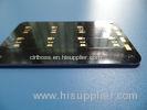
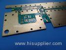
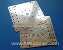
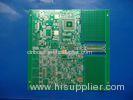
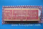
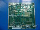
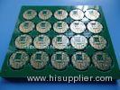
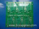
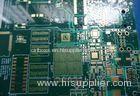
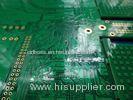
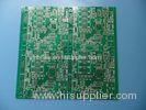
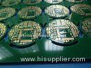
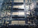
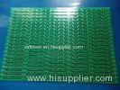
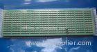
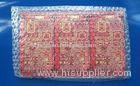
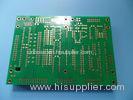
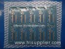
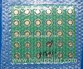
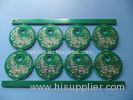
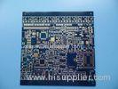
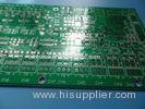
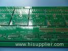
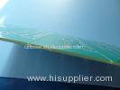
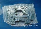
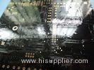
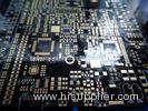
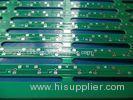
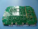
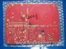
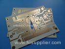
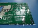
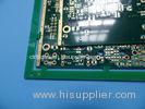
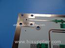
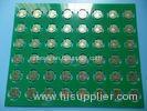
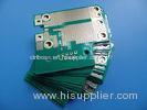
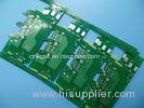
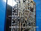
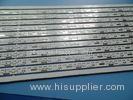
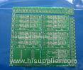
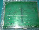
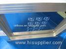
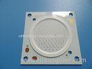
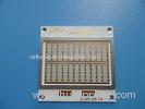
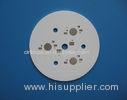
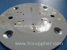
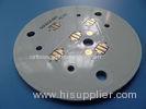
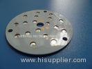
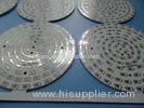
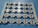
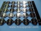
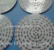
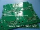
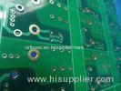
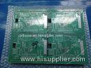
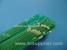
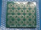
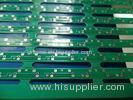
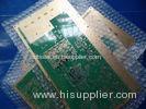
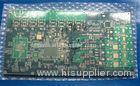
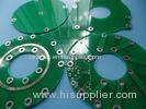
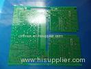
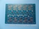
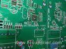
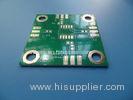
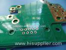
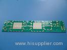
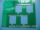
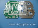
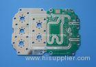
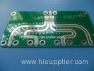
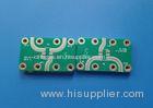
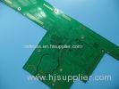
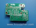
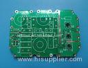
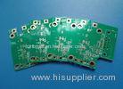
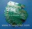
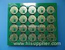
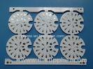
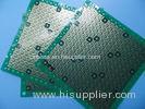
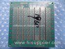
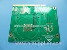
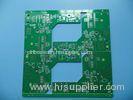
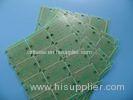
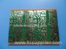
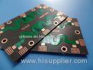
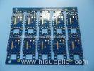
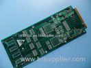
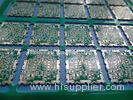
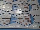
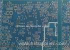
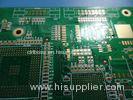
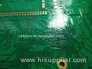
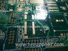
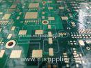
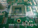
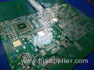
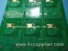
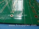
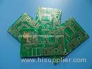
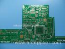
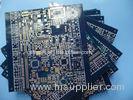
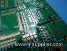
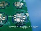
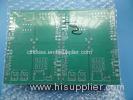
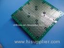
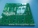
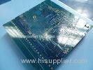
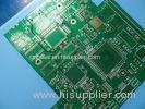
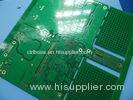
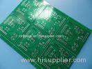
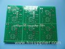
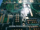
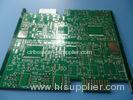
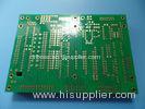
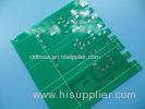
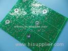
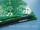
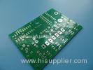
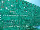
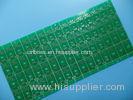
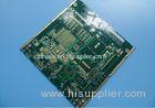
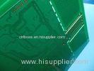
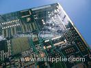
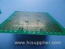
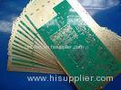
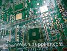
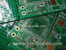
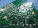
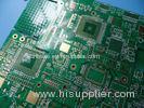
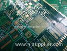
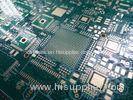
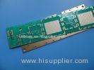
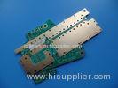
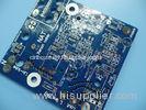
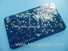
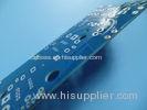
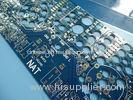
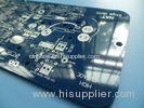
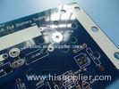
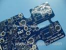
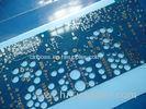
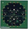
Green 1.5oz Multi Layer PCB Board High Temperature Impedance Controlled
| Place of Origin: | Zhejiang, China (Mainland) |
|
|
|
| Add to My Favorites | |
| HiSupplier Escrow |
Product Detail
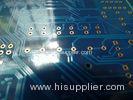
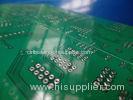
Green 1.5oz Multi Layer PCB Board High Temperature Impedance Controlled
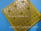
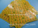
PCB Data sheets
<table border="
Green 1.5oz Multi Layer PCB Board High Temperature Impedance Controlled
PCB Data sheets
| PCB SIZE | 220 x 230mm=1PCS |
| BOARD TYPE | |
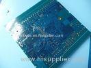
| Number of Layers | Multilayer PCB, 4 Layer PCB |
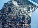
| Surface Mount Components | YES |
| Through Hole Components | YES |
| LAYER STACKUP | copper ------- 35um(1oz)+plate TOP layer |
| 1080 x 2 0.15mm | |
| copper ------- 35um(1oz) | |
| Core FR-4 2.0mm | |
| copper ------- 35um(1oz) | |
| 1080 x 2 0.15mm | |
| copper ------- 35um(1oz)+plate BOT Layer | |
| TECHNOLOGY | |
| Minimum Trace and Space: | 4mil/4mil |
| Minmum / Maximum Holes: | 0.4mm/3.8mm |
| Number of Different Holes: | 12 |
| Number of Drill Holes: | 5015 |
| Number of Milled Slots: | 0 |
| Number of Internal Cutouts: | 0 |
| Impedance Control | Differential pairs impedance control, Layer 1, 5/5mil, 100ohm+/-10% |
| BOARD MATERIAL | |
| Glass Epoxy: | FR-4, ITEQ IT-140 TG>135, er<5.4 |
| Final foil external: | 1.5oz |
| Final foil internal: | 1oz |
| Final height of PCB: | 2.5mm ±0.2 |
| PLATING AND COATING | |
| Surface Finish | Immersion Gold (16.9%) 2µ" over 100µ" nickle |
| Solder Mask Apply To: | Top and Bottom, 12micon Minimum. |
| Solder Mask Color: | Green, LP-4G G-05, Nanya supplied |
| Solder Mask Type: | LPSM |
| CONTOUR/CUTTING | Routing |
| MARKING | |
| Side of Component Legend | TOP |
| Colour of Component Legend | White, S-380W, Taiyo Supplied. |
| Manufacturer Name or Logo: | Marked on the board in a conductor and leged FREE AREA |
| VIA | Plated Through Hole(PTH), via tented. |
| FLAMIBILITY RATING | UL 94-V0 Approval MIN. |
| DIMENSION TOLERANCE | |
| Outline dimension: | 0.0059" (0.15mm) |
| Board plating: | 0.0030" (0.076mm) |
| Drill tolerance: | 0.002" (0.05mm) |
| TEST | 100% Electrical Test prior shipment |
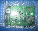
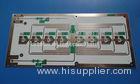
| APPLICATION: | IP Telephony, GPS Trackers Signal Generator Video Surveillance Wireless Bridge CCTV System |
| TYPE OF ARTWORK TO BE SUPPLIED | email file, Gerber RS-274-X, PCBDOC etc |
| SERVICE AREA | Worldwide, Globally. |
Advantages
a) 2.5mm thick PCB, impedance controlled PCB and Immersion gold.
b) PCB manufacturing on required specifications. Right manufacturing instruction (MI), comprehensive equipment management and maintenance and process control, strict WIP inspection and monitoring as well as working instruction, all those make the whole fabrication process totally controlled.
c) DDU Door to door shipment with competitive shipping cost.
d) Meeting your printed circuit board needs from PCB prototyping to mass volume production.
More Applications in Electronics
Rf Amplifier Circuit
Dc Power Converter
Dcdc Converter
Electronics Assembly
Cheap Plc
PCB knowledge: Printed circuit boards
Printed circuit board (short for PCB) is an important electronic part. It is the supporting body of electronic component and the electrical connection supporter of electronic component. Since it’s made by electronic printing, it’s called printed circuit board.
Role
After PCBs are applied in electronic equipment, since it’s consistency of the same board, it confidently avoids the error of manual wiring. PCB can achieve the automatic pick and place or surface mounting, automatic soldering, automatic inspection. It guarantees the quality of electronic equipment. The labor productivity is improved, the cost is reduced and the maintenance is convenient.
Development
Printed circuit board develops from single sided to double sided, multilayer and flexible, and still maintain their own development trends. Due to the continuous development of high precision, high density and high reliability, and constantly reduce the volume, reduce costs, improve performance, making the printed circuit board in the future development of electronic equipment, still maintained a strong vitality.
Review on the future development trend, the manufacturing technology of PCB mainly is consistent, namely high density, high precision, small diameter, thin track, fine pitch, high reliable, multilayer, high-speed transmission, light weight, thin direction. To improve productivity, reduce costs, reduce pollution, adapt to many varieties and small batch production are the production direction at the same time. The technology development level of printed circuit boards, it is regarded with line width, PCB drill, aspect ratio as a representative.
History
The creator of printed circuit board is Austrian engineer Paul Eisler. He invented the printed circuit as part of a radio set while working in England around 1936. In 1943, The USA began to use the technology on military radio. In 1948, the USA released the invention for commercial use. Since the mid-1950s, printed circuits became commonplace in consumer electronics and began to be widely used.
Before PCB, the interconnection between the electronic components is relying on the wires directly connected to complete. Nowadays, only in the laboratory test wire exists. Printed circuit board in the electronics industry has occupied the absolute control status.

FAQ
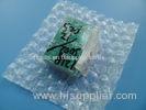
How do you pack the PCBs?
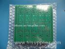
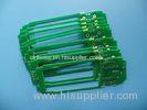
PCBs are packed with Polyethylene air cushion film(vacuum plastic bags) per 20-25 pieces. Pearl cotton (Polyethylene foamed sheet) are put inside carton box.
The hardness of carton box is KK grade(the highest hardness). Maximum gross weight for one carton is less than 12
Related Search
Find more related products in following catalogs on Hisupplier.com
Related Products
Company Info
BICHENG ENTERPRISE LIMITED [China (Mainland)]
Business Type:Manufacturer
City: Shenzhen
Province/State: Guangdong
Country/Region: China (Mainland)