

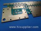
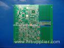
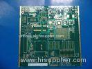
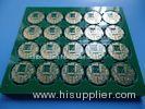
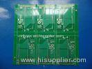
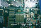
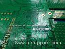
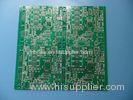
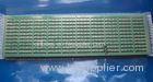
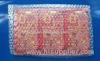
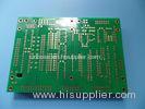
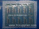
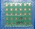
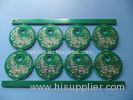
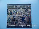
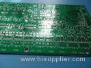
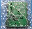
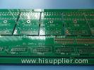
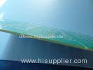
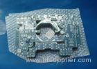
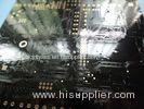
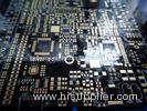
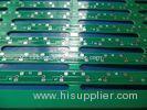
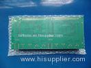
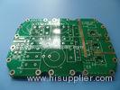
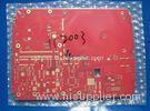
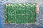
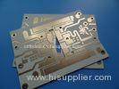
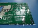
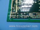
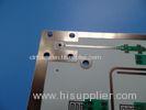
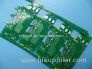
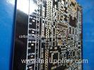
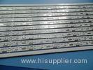
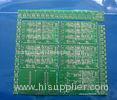
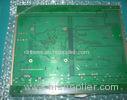
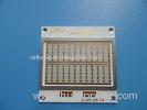
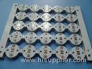
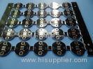
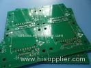
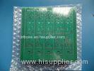
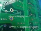
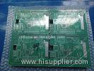
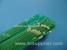
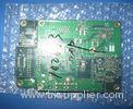
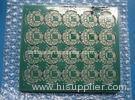
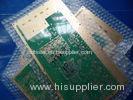
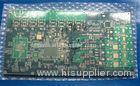
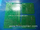
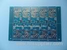
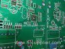
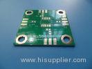
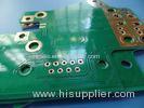
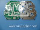
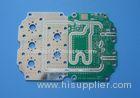
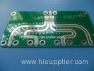
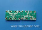
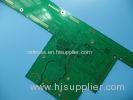
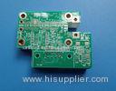
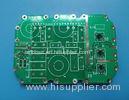
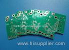
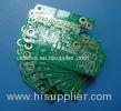
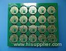
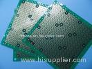
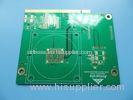
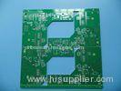
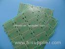
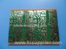
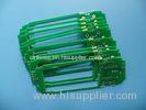
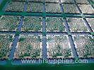
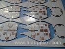
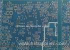
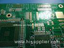
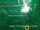
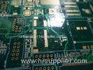
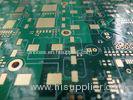
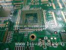
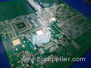
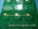
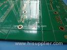
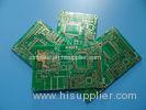
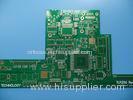
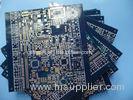
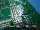
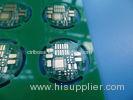
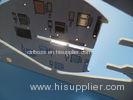
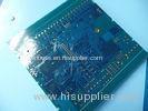
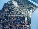
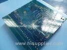
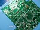
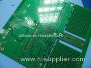
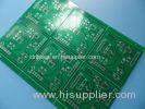
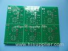
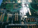
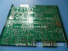
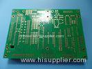
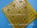
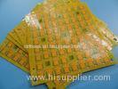
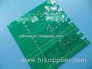
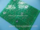
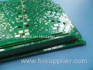
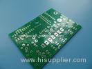
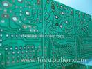
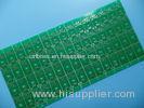
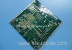
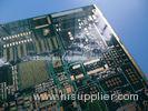
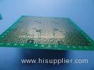
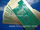
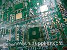
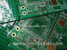
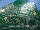
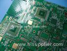
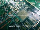
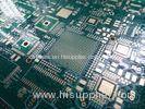
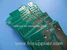
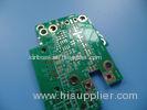
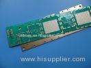
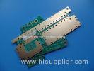
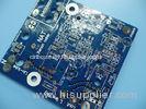
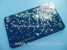
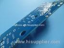
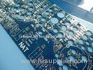
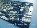
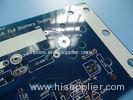
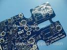
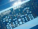
HASL Multilayer Heavy Copper PCB Layout 1oz Printing Circuit Boards
| Place of Origin: | Zhejiang, China (Mainland) |
|
|
|
| Add to My Favorites | |
| HiSupplier Escrow |
Product Detail
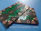
HASL Multilayer Heavy Copper PCB Layout 1oz Printing Circuit Boards
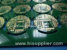
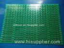
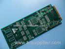
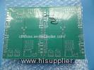
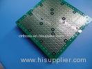
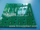
PCB properties
<table border="1" cel
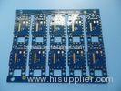
HASL Multilayer Heavy Copper PCB Layout 1oz Printing Circuit Boards
PCB properties
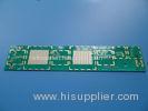
| PCB SIZE | 191 x 74mm=1PCS |
| BOARD TYPE | |
| Number of Layers | Multilayer PCB, 4 layer PCB |
| Surface Mount Components | YES |
| Through Hole Components | YES |
| LAYER STACKUP | copper ------- 18um(0.5oz)+plate TOP layer |
| Prepreg 7628 0.195mm | |
| copper ------- 35um(1oz) MidLayer 1 | |
| FR-4 1.0mm | |
| copper ------- 35um(1oz) MidLayer 2 | |
| Prepreg 7628 0.195mm | |
| copper ------- 18um(0.5oz)+plate BOT Layer | |
| TECHNOLOGY | |
| Minimum Trace and Space: | 6.7mil/6.4mil |
| Minmum / Maximum Holes: | 0.3/3.28mm |
| Number of Different Holes: | 12 |
| Number of Drill Holes: | 5371 |
| Number of Milled Slots: | 0 |
| Number of Internal Cutouts: | 0 |
| Impedance Control: | no |
| Number of Gold finger: | 35 |
| BOARD MATERIAL | |
| Glass Epoxy: | FR-4 TG135, CTI 175V-249V, er<5.4. ITEQ Supplied |
| Final foil external: | 1oz |
| Final foil internal: | 1oz |
| Final height of PCB: | 1.6mm ±0.16 |
| PLATING AND COATING | |
| Surface Finish | Hot Air Soldering Leveling(HASL), Sn>=2.54µm, Electroplated edge connector, 10microinch. |
| Solder Mask Apply To: | TOP and Bottom, 12micron Minimum |
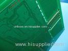
| Solder Mask Color: | Green, PSR-2000GT600D, Taiyo Supplied |
| Solder Mask Type: | LPSM |
| CONTOUR/CUTTING | Routing |
| MARKING | |
| Side of Component Legend | TOP and Bottom. |
| Colour of Component Legend | White, S-380W, Taiyo Supplied. |
| Manufacturer Name or Logo: | Marked on the board in a conductor and leged FREE AREA |
| VIA | Plated through hole(PTH), via tented. |
| FLAMIBILITY RATING | UL 94-V0 Approval MIN. |
| DIMENSION TOLERANCE | |
| Outline dimension: | 0.0059" |
| Board plating: | 0.0029" |
| Drill tolerance: | 0.002" |
| TEST | 100% Electrical Test prior shipment |
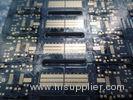
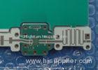
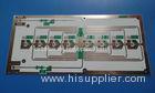
| APPLICATION: | Socket accessories |
| TYPE OF ARTWORK TO BE SUPPLIED | email file, Gerber RS-274-X, PCBDOC etc |
| SERVICE AREA | Worldwide, Globally. |
Advantages
a) FR-4 HASL + edge connector
b) Customer complaint rate: <1%
c) Engineering design prevents problems from occurring in pre production.
d) 100% tests inclusive of electrical test and AOI inspection.High voltage test, Impedance control test, micro-section, solder-ability test, thermal stress test, reliability test, insulation resistance test and ionic contamination test etc.
e) Devlivery on time: >98%
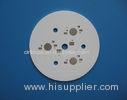
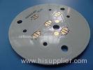
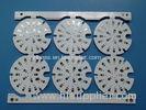
More Applications in Electronics
Embedded Systems Projects
User Access Control
Leds Lights
Microstrip Antenna
Server Blade
PCB knowledge: The components of multilayer PCB --- copper foil
A multilayer board consists of copper foils, thin rigid laminates and prepreg sheets.
The standard thicknesses for copper foils are shown below
| µm | 5 | 9 | 12 | 17.5 | 35 | 70 |
| oz | 0.14 | 0.25 | 0.34 | 0.5 | 1 | 2 |
Thick copper (heavy copper) foils are used for voltage and ground planes by some electronics companies. Thicknesses up to 210 µm (6 oz) are specified for high voltage coil boards. For very fine-line boards, 5 and 9 µm (0.14 and 0.25 oz.), ultrathin copper foils are also used for the outer layers.
Copper foils are used as copper cladding of the thin laminates used in the inner layers. Such laminates can be delivered with different copper thicknesses on the two sides, for example, 17.5 µm (0.5 oz.) on one side for a signal layer and 35 µm (1 oz.) on the other side for ground or voltage planes.
Copper foils are sometimes used directly as cap foils for the outer layers. In such cases, the copper foils are bonded to the next layers by means of prepreg and form the outer layer circuits.
For signal outer layers, the copper foil thickness is usually 17.5 µm (0.5 oz.) or 35 µm (1 oz.) depending on the minimum track width and spacing. In the case of high-density fine-line boards, 5 or 9 µm (0.14 or 0.25 oz.) ultrathin copper foils can be the only solution to achieve the required high resolution when etching the board.
For signal inner layers, a 35 µm (1 oz.) copper foil is normally chosen. For ground and voltage planes, 35 µm (1 oz.) and 70 µm (2 oz.) copper foils can be used. However, the thicker foil, the more difficult it is to fill the apertures in the planes around the hole wall with epoxy flowing from the prepreg sheets during lamination.
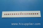
Beveling of Edge connector

FAQ
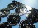
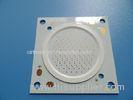
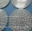
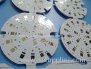
Do you sell MCPCB?
Yes. We offer metal core PCB(MCPCB), single sided and double sided, aluminum core and copper core, 1W/MK, 2W/MK and 3W/MK etc.
Related Search
Find more related products in following catalogs on Hisupplier.com
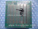
Related Products


Company Info
BICHENG ENTERPRISE LIMITED [China (Mainland)]
Business Type:Manufacturer
City: Shenzhen
Province/State: Guangdong
Country/Region: China (Mainland)
You May Like:


Sitemap XML
About HiSupplier Help Center Customer Service Friend Links Site Map Archives
Browse by: China Suppliers - Hot Products - Products Directory - Offers Directory - Suppliers Directory - Buyers Directory
Language Option: العربية - Nederlands- Français- Deutsch- Italiano- 日本語- 한국의- Português- Pусский- Español
